(1)
Radiation Monitoring Devices Research Nuclear Medicine, Water town, Massachusetts, USA
8.1 Introduction
8.2 Compound Halides
8.3 Alkali Halides
8.3.1 Activated Sodium Iodide
8.4.1 Lead Iodide (PbI2)
8.4.2 Mercuric Iodide (HgI2)
8.4.3 Thallium Bromide (TlBr)
8.6.1 Synthesized LSO
8.10.1 Diamond
8.10.2 Silicon
8.10.3 Silicon Strip Detector
8.10.4 Germanium
Abstract
Since the invention of planar technology, semiconductor radiation detector technology has been developed on planar technology for a wide range of applications in medical imaging, high-energy physics applications, and photon detection. The vertex detectors used in high-energy physics consists of both single-sided and double-sided silicon strip detectors arranged in a cylindrical shape around the beam collision point [1–3]. The success of silicon detectors in position-sensitive particle detection in accelerator experiments was soon used to the ideas of applications in other field of research such as medicine and industry.
8.1 Introduction
Since the invention of planar technology, semiconductor radiation detector technology has been developed on planar technology for a wide range of applications in medical imaging, high-energy physics applications, and photon detection. The vertex detectors used in high-energy physics consists of both single-sided and double-sided silicon strip detectors arranged in a cylindrical shape around the beam collision point [1–3]. The success of silicon detectors in position-sensitive particle detection in accelerator experiments was soon used to the ideas of applications in other field of research such as medicine and industry.
Since digital X-ray imaging system offered several advantages over analog film-based imaging system, immense effort and a lot of money have been invested to develop digital X-ray imager with inorganic scintillating materials (e.g., selenium (Se), mercuric iodide (HgI2), cesium iodide (CsI)) on flat-panel pixelated substrate [4–6].
Small field detectors that may be combined for scanning configurations are mainly based on charge-coupled devices (CCD) [7, 8], but directly converting systems with crystalline semiconductors, CMOS, and bump bonding technology have also been developed [9, 10].
The X-ray imaging system for medical use requires higher X-ray energy, and Z value materials higher than 40 are preferable for high stopping power. The lattice should have a close-packed geometry (such as body-centered cubic) to optimize density. The material should have a low dielectric constant to ensure low capacitance and system noise. From electronic point of view, the band gap energy should be greater than 0.14 to ensure that there is negligible thermal generation of carriers at room temperature, and the resistivity should be greater than 108 Ω-cm to allow larger biases to be applied, resulting in faster drift velocities and deeper depletion depth. Finally, electron and hole mobility-lifetime product (μτ) should be better than 10−2 and 10−3, respectively, to ensure good carrier transport and therefore spectral performance.
According to some observers, CdTe and CdZnTe (CZT) are more promising in medical gamma (γ)-ray imaging than GaAs and HgI2 because of improved spatial and energy resolution [11]. However, recent studies with screen-printed HgI2 films are showing not only promising results but these devices are cost-effective [12, 13].
8.2 Compound Halides
After Roentgen’s discovery of X-rays, the search for detectors to detect the radioactivity in materials became number one priority. As a result, the discovery of the inorganic compound CaWO4 came into the market. In 1940, the discovery of scintillation in naphthalene led to the discovery of thallium-activated sodium iodide (NaI). In 1950, there was a burst of alkali halide compounds that seemed very interesting, and their performance as radiation detectors was investigated. Among them, lithium-containing compounds to detect neutrons are worth mentioning. Activated cesium iodide (CsI:Tl) came afterward along with barium fluoride BaF2. The iodide scintillators like NaI, NaI:Tl, and CsI:Tl have wide emission spectra with maximum ranging from 330 for NaI:Tl to 550 nm for CsI:Tl. The most interesting thing about these two compound halides is their electron response functions that are very much similar in shape but the magnitudes are different [14].
The other compound halides that we will discuss are PbI2, HgI2, TlBr, LaBr3 LaCl3, RbGd2Br7, and LuI3. There are too many inorganic compound halide scintillators that are in the state of developments. It is not possible to include each and every one of the scintillators.
Both mercuric iodide (HgI2) and lead iodide (PbI2) have high atomic numbers which is one of many characteristics of a scintillating material used as a radiation detector. Mercuric iodide (HgI2) has received the attention of solid-state physicists because of its optical properties, especially the excitonic effects in correspondence of the fundamental absorption edge and interesting photoconductive properties. In 1971, Willing and Roth first pointed out that red variety of HgI2 is a good material for radiation detector because of its high atomic number (80/53), large band gap (~2.2 eV), and low electron–hole pair creation energy (~4.2 eV) [15]. Lead iodide (PbI2) on the other hand has comparable atomic number (82/53) and band gap (2.3 eV), but requires more energy (~8.4 eV) to create electron-hole (e-h) pair. However, the e–h pair creation energy depends on the quality of the grown crystals (both HgI2 and PbI2).
Thallium bromide (TlBr) has almost all the properties that should be possessed by a scintillating material to be used as a radiation detector. It has wide band gap (2.68 eV) and high atomic number (81/35), so the Fano noise has low and high resistivity (1012 Ω-cm), meaning larger bias can be applied resulting in faster drift velocities and deeper depletion depth. However, from the graph, we can see that the compound halides such as HgI2, PbI2, and TlBr are displaced from the line of other bulk semiconductors giving a 30 % reduction in mean pair creation energy for a given band gap compared to main branch (Fig. 8.1) [16].
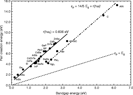
Fig. 8.1
The energy required for creating e–h pair as a function of band gap energy (Reproduced after Owens and Peacock, with permission, Elsevier Pub.)
Both LaBr3:Ce and LaCl3:Ce doped have high light yield (≥50,000 and 40,000 ph/MeV), fast response, and good energy resolution. On the other hand, LuI3 Ce3+ has also shown high light yield, fast response, and good energy resolution [17].
The cerium-activated (with 10 % cerium) rubidium gadolinium bromate (RbGd2Br7:Ce), the new cerium-doped halide scintillator has a very high light output (56,000 photons/MeV) almost comparable to LaBr3:Ce and LaCl3:Ce, a very good linearity in energy response and over a wide range of energy, and fast principle decay constant (43 ns) [18].
8.3 Alkali Halides
8.3.1 Activated Sodium Iodide
Activated sodium iodide (NaI) with thallium (Tl) has been used as a gamma (γ)-ray detector for a long time. The Tl concentration is maintained about 10−3 mole fraction. As a matter of fact, thallium-doped sodium iodide (NaI:Tl) material is the most widely used scintillation material in spite of three decades of research and development of several new scintillating materials. NaI:Tl scintillating material is used traditionally in nuclear medicine, environmental measurements, geophysics, and medium-energy physics. NaI:Tl crystals are also used to manufacture X-ray detectors of high spectrometric quality with increased thallium concentration.
The high light output, convenient emission range coincident with maximum efficiency region of photomultiplier tube (PMT) with bi-alkali photocathodes, no significant self-absorption of the scintillated light, the possibility of large size production of single crystals, and their low cost and toxicity compared to the other scintillation materials mainly compensate to a great extent for the main thallium-doped sodium iodide (NaI:Tl) crystals disadvantage, namely, the hygroscopicity.
Some of the properties of NaI (Tl) are given below:
Properties of thallium-activated sodium iodide (NaI:Tl)
Afterglow = approx. 4 % after 2 ms and 8 % after 1 ms
Cleavage planes = <100>
Decay constant (μs) = 0.23
Density (g/cm3) = 3.70
Spectral emission range (nm) = 325–525
Gamma and X-ray absorption coefficients (cm−1) = 0.29 at 660 keV and 5.5 at 100 keV
Light escape cone to air (0°) = 44.7
Light escape cone to glass (0°) = 56.5
Light escape from one face to air (%) = 8.4
Light escape from one face to glass (%) = 22.4
Melting point (°C) = 651
Optical transmission range = 250 nm–35 μm
Peak scintillation wavelength (nm) = 410
Photons/MeV = 40,000
Radiation length (cm) = 2.59
Refractive index at peak emission = 1.80
Structure = bcc
Stability = very hygroscopic
Temperature coefficient of light output (%K−1) = 3.47 at 298 K
1.
Emission Spectra of Activated NaI: Emission spectra of NaI:Tl under study are measured at room temperature, irradiating the sample with an X-ray beam characterized by a mean energy of 30 keV (peak energy at 50 keV) and an intensity of 2 kRad/min. The single crystal of NaI:Tl doped (0.001 mole fraction) and grown by Bridgman–Stockbarger (B–S) method shows a broad peak around 420 nm, corresponding to the thallium (Tl) emission. The hump in the shoulder around 480 nm is presumed to be due to impurities (Fig. 8.2) [19].
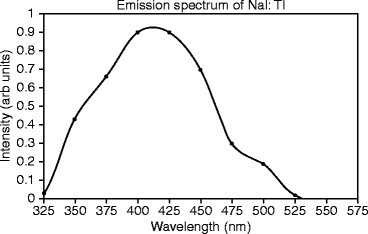
Fig. 8.2
The emission spectrum of thallium-activated sodium iodide (NaI:Tl)
Thallium-activated sodium iodide (NaI) is notable for high light yield (more than 40,000 Photons/MeV) at room temperature, and about 25 eV is required to produce single photon. The light yield is maximum at room temperature (~27 °C). However, light yield significantly reduces below 0 °C and above 60 °C (Fig. 8.3). Lowering of temperature leads to the deterioration of monocrystal self-resolution caused by inhomogeneity of light yield. It has been observed that activator concentration also affects the temperature dependency of the light output to some extent [20].
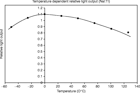
Fig. 8.3
A typical temperature-dependent light output plot of a single crystal NaI:Tl
The high concentration of thallium (higher than 0.1 mole fraction) in sodium iodide crystal influences the excitation and luminescence spectra of the crystal and ultimately the energy spectra due to the transfer of the absorbed energy in the dimmer bands [21].
2.
Absorption Phenomenon in Activated NaI: At a temperature less than 80 K, NaI:Tl shows four (A, B, C, and D) absorption bands at 285, 253, 245, and 210 nm, and at liquid helium temperature excitation in the A, B, and C bands of NaI:Tl produces two emission bands at 330 and 420 nm [22, 23].
The graph (Fig. 8.4) is based on the calculations of the exponential function for certain values of x (thickness) for NaI. The number of photons absorbed by a certain thickness of the absorber is calculated on the basis of the ratio of [(I 0/I)/I 0], where I 0 is the initial intensity of photons and I is the intensity after being traveled through the absorber. From the above graph, we can say that NaI crystal of quarter of an inch thick will absorb ~20 % of the 500-keV photons incident on its surface.
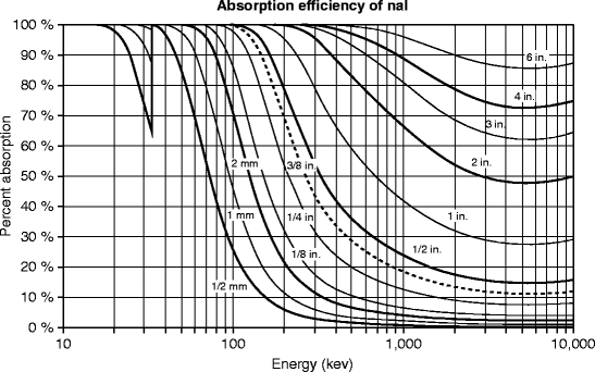
Fig. 8.4
The absorption efficiency of NaI:Tl at room temperature (Courtesy of Saint-Gobain Crystals)
3.
Electron Energy Resolution in Activated NaI: At high-energy excitation, the self-trapped excitons’ emissions at 295 nm are observed in addition to the activator bands. In order to account for transport of carriers and excitons, in terms of how they transfer energy to the activators with competition from non-radiative decay pathways, several theories and experiments have been put forward by several investigators [24, 25].
The incident gamma (γ) ray on the scintillator produce fast electrons, and the photon energy resolution is the convolution of electron spectrum. The final signal produced by the photomultiplier (PM) dynodes as a result of multiplication depends on the total number of photons produced by the scintillator (considering the non-proportionality), the total photoelectron collection by the cathode, and the photoelectrons collected by the first dynode. Though there are several papers on the non-proportional light yield (Fig. 8.2), which ultimately affects the energy resolution of thallium-activated NaI, the science is still not well understood.
Figure 8.5 shows thallium-activated NaI electron energy resolution η e measured following modified Compton coincidence technique (MCCT) [25]. The activated sodium iodide crystal is coupled to two PMTs for dark current reduction. The electron energy deposited on NaI:Tl crystal was determined by subtracting scattered energy from the source energy (662 keV). Non-proportionality is noticed to be minimum in strontium iodide (SrI2) doped with europium (Eu). The thallium-doped NaI shows almost double amount of non-proportionality compared to Eu-doped SrI2 [24] while offering very high light output (~100,000 photons/MeV).
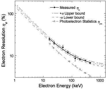
Fig. 8.5
Electron energy resolution in thallium-activated NaI (Reproduced from [25], with permission from IEEE)
4.
Decay Constant of Thallium-Activated NaI: The most notable property of NaI:Tl is its high excellent light yield property, but the dominant decay time of scintillation pulse of 230 ns is not comfortable for a scintillating material when high speed is the main criterion.
In addition to the excellent light yield, phosphorescence with characteristic of 0.15 s decay time has also been measured in NaI:Tl crystal, which contributes 9 % to the overall light yield [26].
The decay time measurements are performed by irradiating the NaI:Tl single crystal with an X-ray beam of mean energy 10 keV. Aluminum foil is used to reduce the presence of soft X-ray in the beam. The calculated rise time and the decay time (τ) calculated from the decay time signal (Fig. 8.6) are 49 and 250 ns, respectively. The temperature-dependent decay time is measured and presented in Fig. 8.7. When increasing the temperature, the decay time decreases very sharply up to 150 ns at 80 °C and then slowly to 100 ns. NaI:Tl exhibits several decay time constant components. As temperature increases, the longer time constant components decrease in intensity.
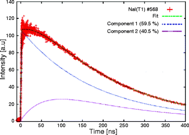
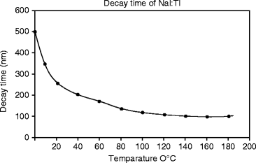
Fig. 8.6
Decay time signal of NaI:Tl single crystal (Reproduced after Mengesha et al, with permission from IEEE)
Fig. 8.7
Temperature-dependent decay time constant (τ) in NaI:Tl crystal
In addition to the excellent light yield, phosphorescence with characteristic of 0.15 s decay time has also been measured in NaI:Tl crystal, which contributes 9 % to the overall light yield [26].
8.3.2 Cesium Iodide (CsI)—Cesium Iodide (CsI) Activated with Either Thallium (Tl) or Sodium (Na)
Cesium iodide (CsI) is another alkali halide scintillating material and has been known since 1950 [27]. The crystal exhibits two emission bands of 290 and 338 nm with decay constants of 0.1 and 0.7 μs, respectively. At room temperature, the CsI crystal exhibits a wide (~50 nm) emission band at 305 nm with decay constants of 10 and 36 ns, and the CsI/NaI:Tl light output ratio is measured between 0.05 and 0.08 for various samples [28]. Commercially CsI is available with thallium (Tl) or sodium (Na) as activator, and different scintillator properties are observed in two cases.
The emission spectra of CsI crystal and doped crystals (Tl and Na) are shown in Fig. 8.8. The undoped crystal shows the maximum peak around 315 nm, whereas the sodium (Na)- and the thallium-doped crystals show maximum peaks approximately at 420 and 550 nm, respectively.
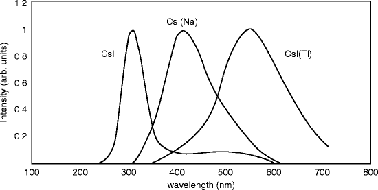
Fig. 8.8
The emission spectrum of CsI and doped (Tl and Na) CsI crystals (Courtesy: SCIONIX)
Both the peaks of the doped crystals are broader in comparison with the undoped crystal. The broad peak of the Tl-activated crystal around 550 nm does not match well to the sensitivity of a (bi-alkali) photocathode of a photomultiplier tube (PMT). As a result, the photoelectron yield for gamma (γ) rays amounts ~45 % of the value of NaI:Tl. However, CsI:Tl scintillation is very well matched with silicon PIN photodiodes, yielding a wavelength-averaged internal quantum efficiency (QE) of approximately 90 % and external QE of about 70 % [29]. On the other hand, the sodium-activated crystal has a peak around 420 nm and is well matched with a (bi-alkali) photocathode of a PMT. Therefore, the photoelectron yield for γ-rays accounts almost 85 % of that of NaI:Tl. However, the photofraction of Tl-doped CsI is higher than Tl-doped NaI because of its higher Z value.
CsI:Tl-doped material shows highest gamma-ray absorption coefficient per unit size of any scintillator. It is less brittle than NaI:Tl and thus can withstand more mechanical shock and vibration, and the crystals combine the advantages of high stopping power and high reliability for large thickness, good energy resolution, and the possibility of light particle isotopic identification using the pulse shape discrimination technique. CsI:Tl has variable decay time for various exciting particles, and thus pulse shape discrimination techniques can be used to differentiate among various types of radiation. The material is less hygroscopic than NaI:Tl. Table 8.1 shows some of the scintillator crystals’ data.
Table 8.1
Some of the data of the scintillator crystals used in medical imaging
Material | NaI:Tl | CsI:Tl | CaF2:Eu | BaF2 | BGO | YAG:Ce | YAP:Ce | GSO:Ce |
|---|---|---|---|---|---|---|---|---|
Chemical formula | NaI:Tl | CsI:Tl | CaF2:Eu | BaF2 | Bi4(GeO4) | Y3Al5O12 | YAlO3 | Gd2SiO5 |
Density (g/cm3) | 3.67 | 4.51 | 3.18 | 4.89 | 7.13 | 4.57 | 5.37 | 6.71 |
Hardness (Moh) | 2 | 2 | 4 | 3 | 5 | 8.5 | 8.6 | 5.7 |
Hygroscopic | Yes | Slightly | No | No | No | No | No | – |
Crystal structure | Cubic | Cubic | Cubic | Cubic | Cubic | Cubic | Rhomb | Mono |
Thermal expansion (ppm) | 47.5 | 50 | 19.5 | 18.4 | 7.0 | 8–9 | 4–11 | 4–12 |
Melting point (C) | 651 | 621 | 1,360 | 1,280 | 1,050 | 1,970 | 1,875 | |
Integrated light output (%NaI:Tl) | 100 | 45 | 50 | 20/2 | 15–20 | 15 | 40 | 20–25 |
Wavelength of maximum emission (nm) | 415 | 550 | 435 | 325/220 | 480 | 550 | 370 | 440 |
Decay constant (ns) | 230 | 900 | 940 | 630/0.6 | 300 | 70 | 25 | 30–60 |
Afterglow (% at 6 ms) | 0.5–5 | <2 | <0.3 | – | <0.005 | <0.005 | <0.005 | <0.005 |
Radiation length (cm) | 2.9 | 1.86 | 3.05 | 2.03 | 1.1 | 3.5 | 2.7 | 1.38 |
Photon yield at 300 K-103pH/MeV | 38 | 52 | 23 | 10 | 2–3 | 8 | 10 | 8–10 |
The cesium iodide (CsI) when activated with sodium (Na) shows higher light output and shows two decay components at 0.46 and 4.18 μs [30]. Table 8.2 shows the properties of cesium iodide (CsI) scintillators without and with activators (Na and Tl).
Table 8.2
Properties of cesium iodide scintillator (activator)
Scintillator (activator) | CsI | CsI (Tl) | CsI (Na) |
|---|---|---|---|
Density (g/ml) | 4.51 | 4.51 | 4.51 |
Hygroscopic | Slightly | Slightly | Yes |
Emission wavelength (nm) | 315 | 550 | 420 |
Lower cutoff | 260 | 320 | 300 |
Refractive index | 1.95 | 1.79 | 1.84 |
Primary decay time μ-s | 0.016 | 1.0 | 0.63 |
Light yield photons/MeV | 2 × 10³ | 54 × 103 | 42 × 103 |
Crystal structure | Cubic | Cubic | Cubic |
Figure 8.9 shows the energy-dependent percentage absorption in CsI:Tl crystal. It has been found that thallium-activated cesium iodide (CsI:Tl) crystal is an efficient absorber of gamma (γ) rays, with a radiation length of 1.65 cm at 662 keV.
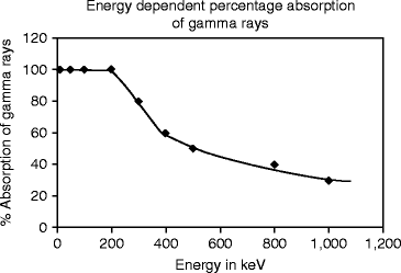
Fig. 8.9
The energy-dependent percentage absorption in CsI:Tl scintillator
The measured absorption with the energy of the gamma ray further shows that absorption is almost 100 % up to the energy of 200 keV. With further increase of energy, the absorption falls very rapidly until the energy reaches 400 keV. After 400 keV the variation in absorption of gamma (γ) ray is almost exponential.
Figure 8.10 shows the electron energy response of CsI crystal activated with thallium (Tl) and sodium (Na). The energy response curve (top) of thallium-activated NaI is also given for comparison. The Compton coincidence technique (CCT) has been implemented for the purpose of photon response in activated cesium iodide to the energy of the incident gamma (γ) ray. For comparison, the response of the photon in activated sodium iodide (NaI) is also given. The photon response, which is defined as the ratio of the light yield to the energy deposited by the photon, has a maximum peak at about 10 keV and then monotonically decreases by about 20 % as the photon energy increases from 10 to 440 keV. Below 10 keV, the photon yield decreases very sharply with decreasing incident energy. Accurate CCT measurements are difficult below 4.0 keV due to interfering thermal noise of the photomultiplier tube (PMT). The convolution measurements of the electron response to discrete energies ranging from the lowest energy (0.71 keV for CsI) to the largest photon energy (typically 2 MeV) are made. The results shown above are from the CCT measurements, and it agrees well (almost 85 %) with the calculated data of Gwin and Murray [32, 33].
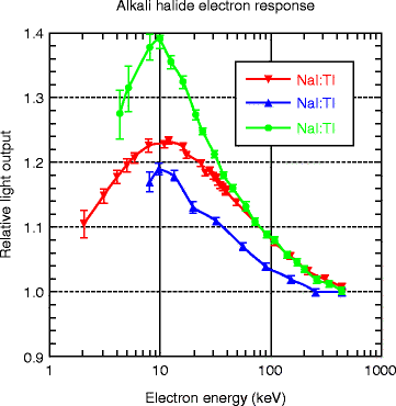
Fig. 8.10
The electron energy response of activated (Tl 2nd and Na 3rd) CsI crystal. The energy response curve (top) of thallium-activated NaI is also given for comparison (Courtesy of Mengesha et al. [31], with permission from IEEE)
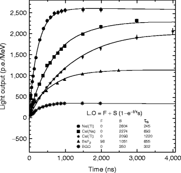
Figure 8.11 shows the light output of doped cesium iodide with other inorganic scintillators as a function of the integration time which is plotted by fitting the following equation [34]:

where F and S are the fast and slow components of the scintillation light and τ d is the decay time constant. The number gamma-ray-excited decay modes for thallium- and sodium-activated cesium iodide (CsI) have slow and fast modes at room temperature [35].
(8.1)
Fig. 8.11
The comparative light output of doped CsI with other inorganic scintillators as a function of the integration time (Courtesy of Mao et al. [34], reproduced with permission from IEEE)
At room temperature, the fast decay time (τ d1) constant is approximately 679 ± 10 ns (63.7 %) and slow decay time (τ d2) constant is approximately 3.34 ± 0.14 μs (36.1 %). The observed (τ d1) luminescent state is populated by an exponential process with a rising time constant of 19.6 ± 1.9 ns at room temperature. In thallium-activated CsI, the longer component has a significant effect on pulse processing and energy resolution and light yield [36]. For excitation with highly ionizing particles, such as α-particle or protons, the ratio between the intensities of these two decay components varies as a function of the ionizing power of the absorbed particle.
The scintillation light yield is dependent on the molar concentration of thallium iodide. However, decay time of CsI(Tl) does not show any such relation with the concentration of thallium in cesium iodide crystals. According to Grassman et al. [37], energy efficiency of CsI(Tl) crystal is higher compared to NaI(Tl) crystal. It has been found that 1-MeV energy was absorbed within NaI(Tl) crystal to generate 4 × 10⁴ photons, whereas the same energy generates 4.5 × 10⁴ photons in CsI(Tl) crystal. Unfortunately, the afterglow in activated CsI is very high, almost 5 % after 3–6 ms which significantly limits the counting rate.
Figure 8.12 shows afterglow in CsI crystals. Crystal nos. 1 and 2 are activated with Tl and Na, respectively, and crystal no. 3 is not activated with any dopant. For comparison, afterglow for zinc tungstate (ZnWO4) and cadmium tungstate is also plotted on the same graph. Afterglow is thought to be due to some deep traps within the crystals (>0.4 eV) which have their glow at temperature >200 K [38]. In order to minimize the afterglow effect, some special co-doping is necessary. Recently co-doped activated cesium iodide with samarium (Sm) has been used to suppress the afterglow effect. The model suggests that Sm electron traps scavenge electrons from thallium traps and that electrons subsequently released by Sm recombine non-radiatively with trapped holes, thus suppressing afterglow [39]. Similar co-doped experiment has been done with NaI:Tl by N.Shiran et al. They found that when the thallium-activated NaI crystal was doped with europium (Eu), it showed increased light yield with shaping time growth [40].
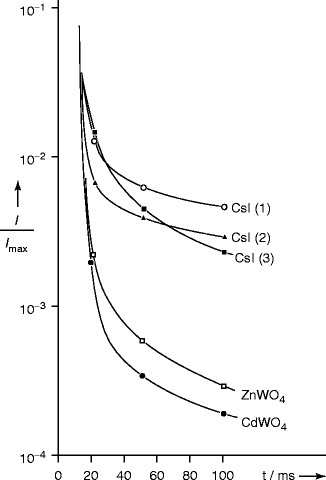
Fig. 8.12
Afterglow in CsI crystals when compared to ZnWO4 and CdWO4 crystals. Crystal nos. 1 and 2 are activated with Tl and Na and no.3 has no dopant
A charged particle passing through a scintillator forms a large number of electron–hole (e–h) pairs. There are several reasons that the total number of e–h pair created cannot be captured because of impurity sites or an activator site. These impurity sites or activator sites capture some of these electrons. For the second case, radiationless transitions are possible between some excited states formed by electron capture and the ground state, in which case no visible photon results. Such processes are called quenching.
The differential quenching efficiency of CsI (Tl) can be expressed as a function of scintillation efficiency and quenching factors as
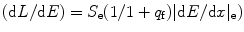
where S e is scintillation efficiency, q f is quenching factor, and (dE/dx)e is electronic stopping power, which is also called nuclear recoil charge density (dE/dx).
(8.2)
The stopping power (dE/dx) = e s + n s = e s (1 + e n/e s), and when it is multiplied by crystal density ρ, it gives rise to stopping power per unit length. The scintillation light output is expected to be reduced (quenched), while timing profile of the pulse is different relative to some energy deposition by maximum ionizing particles [41–43]. The cesium iodide (CsI) when activated with sodium (Na) shows higher light output and shows two decay components at 0.46 and 4.18 μs [30]. Figure 8.13 shows the quantum efficiency of a thallium-activated CsI crystal.
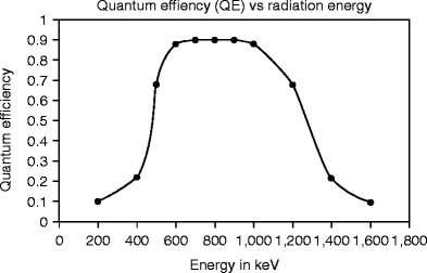
Fig. 8.13
The quantum efficiency of a thallium-activated CsI crystal
Cesium iodide also has a useful property when grown by special technique in thin layers on specially prepared substrates. The deposited material can be formed columnar to make channels for the light to pass through them very easily. The gap between the columns is filled with reflective coating to minimize loss or cross talk between the columns.
Vacuum-Deposited Columnar Film: Hot-wall epitaxial (HWE) technology has been very popular in semiconductor industries and has been used to grow columnar-structured thallium (Tl)-activated cesium iodide film to maximize light output from the film. These films have excellent spatial resolution and high detection efficiency and have been used in gamma (γ)-ray detector, medical imaging system, nondestructive testing (NDT), astronomy, and macromolecular crystallography [44, 45]. Figure 8.14 shows the picture of a columnar-structured film grown by hot-wall epitaxial technology. The 2,000-μm-thick columnar-structured film preserves film light output maximum ensuring excellent optical transmission and good spatial resolution. Filling the gap between the columns with an appropriate reflective material increases the light output by 80 %.
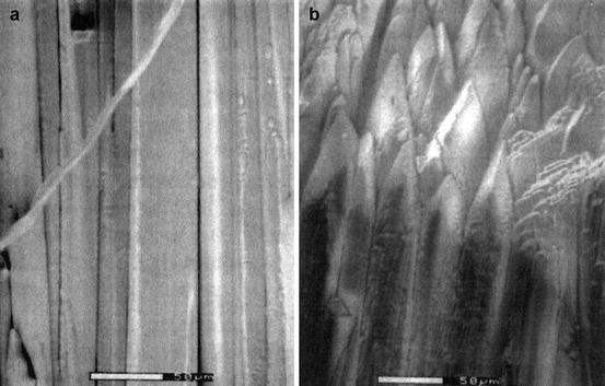
Fig. 8.14
The picture of a columnar-structured film of CsI:Tl
Figure 8.15 shows the light output conversion efficiency of a CsI:Tl vacuum-deposited plate after reflective and absorptive coatings. The luminescence properties of these columns differ from those of CsI (Tl) scintillation crystals without coatings [46]. In addition to the standard emission bands at 400 nm (Tl emission) and 550 nm (strongly perturbed thallium-bound excitation emission), an additional band is observed at 460 nm at liquid nitrogen temperature, which is attributed to a weekly perturbed thallium-bound excitation center [47].
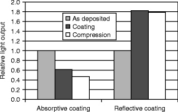
Fig. 8.15
Light output conversion efficiency of a CsI:Tl vacuum-deposited plate after reflective and absorptive coatings
The modulation transfer function (MTF) of a 150-μm film is measured for spatial frequencies in the range of 0–12 lines per millimeter, and calculations are done by following fast Fourier transform (FFT). The detector is exposed to a flood field of 30-kV W X-rays. The isostatically compressed (30 Kpsi) film shows the highest percentage MTF compared to untreated and treated film (Fig. 8.16).
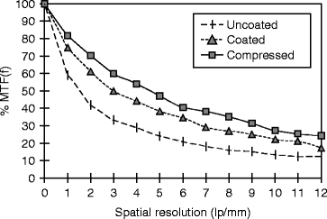
Fig. 8.16
The spatial resolution versus % modulation transfer function (MTF) of CsI(Tl) films
8.4 Halides of Heavy Metals
In this section, we will discuss mostly the heavy metals of halides and metals that have tellurium in the metal matrix. These compounds are semiconductor materials and can be called photoconductors. These materials convert X-ray energy directly to electrical signal. In section 5B.1 we have discussed two alkali halides, namely, NaI and CsI. These two materials are scintillation material and convert energy of X-ray to photons to visible light. According to the principles of operations of the radiation detectors, they are classified as indirect and direct radiation detectors.
Figure 8.18 (a) and (b) show the schematic of the working principle of the indirect and direct scintillators; (c) and (d) are the schematic of the actual arrangements of the scintillators and the electronic circuitry. The fabrication of room temperature nuclear radiation detectors requires a semiconducting material that has high atomic number (Z) for efficient radiation or atomic interaction, large enough band gap for high resistivity, and low leakage currents. In addition, the material should have small band gap so that the electron–hole (e–h) ionization energy is small (<5 eV). Finally, the device (scintillator/radiation detector) fabricated out of the material should have high intrinsic μτ product, high purity, homogeneous, and defect-free which can be matched with a proper ohmic contact electrodes [50].
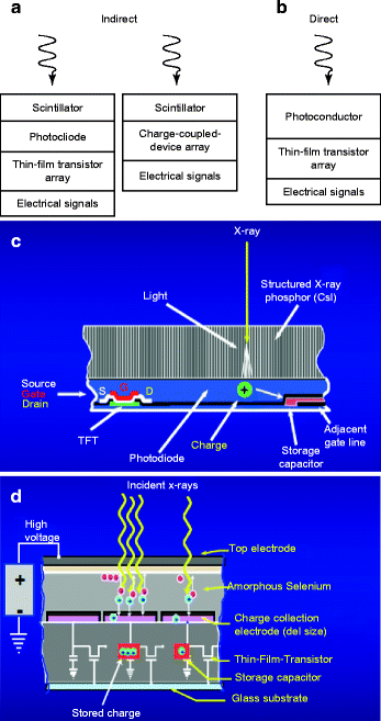
Fig. 8.18
(a, b) Schematic of indirect and direct working principle of the scintillators. (c, d) Schematic of the actual arrangements of the scintillators and the circuitry (Courtesy: J.A. Scipert, UC, Davis)
Table 8.3 shows the band gap, the μτ product, the resistivity, and the absorbed ionizing radiation energy required to create electron hole pairs (e–h) in different compound semiconductors we are interested in, for example, lead iodide (PbI2), mercuric iodide (HgI2), cadmium telluride (CdTe), and cadmium zinc telluride (CZT) and thallium bromide (TlBr). Later on we will also discuss some elementary semiconductors like silicon (Si) and germanium (Ge) that are used as radiation detectors and their pros and cons.
Table 8.3
Some of the properties of compound semiconductors
Material | Atomic number | Density (g/cm3) | Band gap (eV) | E pair (eV) | Resistivity (Ω-cm) | μτ (e) product (cm2/V) | μτ (h) product (cm2/V) |
|---|---|---|---|---|---|---|---|
PbI2 | 82, 53 | 6.2 | 2.32 | 4.9 | 1012 | 8 × 10⁻⁶ | ~10−5 |
HgI2 | 80, 53 | 6.4 | 2.13 | 4.2 | 1013 | 10−4 | 4 × 10⁻⁵ |
TlBr | 81, 35 | 7.56 | 2.68 | 6.5 | >1010 | 10−3 | 4 × 10⁻⁵ |
CdTe | 48, 52 | 6.2 | 1.44 | 4.43 | 109 | 3 × 10⁻³ | 2 × 10⁻⁴ |
CdZnTe | 48, 30, 52 | 6.0 | 1.5–2.2 | ~5.0 | >1010 | 3 × 10⁻³ | 10−5 |
The charge collection efficiency (η) of a photoconducting insulator is given by Hecht’s equation [51]:
![$$ \eta =(\mu \tau E)/L\ [1-\exp (-L/\mu \tau E)] $$](/wp-content/uploads/2017/03/A308734_1_En_8_Chapter_Equ00083.gif)
where μ is mobility of the carriers, τ is bulk trapping or recombination time, E is the electric field applied, and L is the length of the photoconducting detector. Experimentally, the μτ product is extracted from the measured field of half-maximum charge collection E mcc in the collected charge versus electric field plot. However, when these charges are collected near the surface, surface recombination of charge carriers sets in, in addition to the bulk trapping [52]. Therefore, Hecht’s equation must be corrected for a near-electrode (near surface) carrier generation to take account of the surface recombination. As a result, the Eq. (8.3) will be modified as
/L\ [1-\exp (-L/\mu \tau E)] $$](/wp-content/uploads/2017/03/A308734_1_En_8_Chapter_Equ00084.gif)
where s is the surface recombination velocity of the corresponding charge carrier. The transport kinetics of holes and electrons will be different when negative or positive polarity is applied to the irradiated electrode. The other important parameter is the de-trapping time of the carrier, which will affect the transient time across the sample and thereby the voltage signal. Assuming that the carrier de-trapping times are long compared to their transit time t t = (L/μE) across the detector, the voltage signal V s can be expressed mathematically as
![$$ {V_{\mathrm{s}}}=\left\{ {\begin{array}{*{20}{c}} 0 \hfill & {t<0} \hfill \\ {\{({Q_0}L/A{\varepsilon_0}{\varepsilon_{\mathrm{r}}})\}\cdot \{1/(1+s/\mu E)\} \cdot \{\tau /{t_{\mathrm{t}}}(1-\exp (-{t_{\mathrm{t}}}/\tau )\}} \hfill & {0<t<tt} \hfill \\ {\{({Q_0}L/A{\varepsilon_0}{\varepsilon_{\mathrm{r}}})\}\cdot \{1/\ (1+s/\mu E)\}\cdot \{\tau /{t_{\mathrm{t}}}(1-\exp\ (-{t_{\mathrm{t}}}/\tau )\}} \hfill & {t>{t_{\mathrm{t}}}} \hfill \\ \end{array}} \right. $$
” src=”/wp-content/uploads/2017/03/A308734_1_En_8_Chapter_Equ00085.gif”></DIV></DIV><br />
<DIV class=EquationNumber>(8.5)</DIV></DIV>where <SPAN class=EmphasisTypeItalic>Q</SPAN> <SUB>0</SUB> is the total charge collected, <SPAN class=EmphasisTypeItalic>ε</SPAN> <SUB>0</SUB> is the permittivity of free space, <SPAN class=EmphasisTypeItalic>ε</SPAN> <SUB>r</SUB> is the relative dielectric constant of the detector, and <SPAN class=EmphasisTypeItalic>A</SPAN> is the area of the detector. The ratio of the induced charge (<SPAN class=EmphasisTypeItalic>Q</SPAN>) to the total charge collected (<SPAN class=EmphasisTypeItalic>Q</SPAN> <SUB>0</SUB>) at the electrode is dependent on a number of parameters as follows [<CITE><A href=]() 53]:
53]:
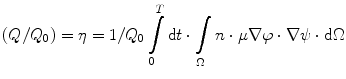
where n is the free electron density, ϕ is the applied bias, ψ is the weighting function, and T is the time interval.
Get Clinical Tree app for offline access

(8.3)
(8.4)
(8.6)
The other important parameter that should be considered as a quality factor of a radiation detector is the energy resolution. Sometimes, we observe broadening of the energy spectrum or shift in the peak of the energy spectrum. The cause of the broadening of the spectrum or shifting of the peak is attributed not only to the poor charge collection but also to electronic noise (Fano noise, noise due to leakage current, and noise due to carrier trapping or polarization). In addition, compound semiconductors have wide range of band gaps, and the resistivities are also higher than the elementary semiconductors. As a result, these compound semiconductors show minimum leakage current [16, 54]. These compound semiconductors thus minimize most of the noise that are not possible to eliminate in elementary semiconductors. As for example, in cadmium zinc telluride (CZT), it has been possible to optimize the noise performance by alternating the zinc (Zn) fraction in the compound semiconductor where the range of possible alloys moves along the line between CdTe and ZnTe due to alteration of Zn.
8.4.1 Lead Iodide (PbI2)
The development of digital (pixelated) radiation detectors that are used in X-ray and gamma (γ)-ray spectrometers and medical imaging system has prompted interest in semiconductors that may function as direct converters, by passing the radiation source to optical photon conversion process. Lead iodide (PbI2) is one of the many materials that has shown promising results and has attracted the attention of the medical professionals and the scientists practicing in medical imaging and radiation therapy. Its properties include high atomic number (82, 53), wide band gap (2.3 eV), low melting point, and adequate charge carrier capabilities (μτ product ~10−5 cm2/V) as we can see from the Table 8.6.
Recent result shows that the radiographic and memographic sensitivities at 72-kVp and 26-kVp measurements, respectively, for a physical vapor-deposited (PVD) polycrystalline PbI2 film are 20 × 106 and 2 × 10⁶ e/mm2/mR, respectively [55]. However, the line-spread function (LSF) with PbI2 crystal degrades with increasing thickness, and the image lag is higher compared to HgI2 film [56]. The long image lag has been attributed to deep impurity states in the forbidden gap of the photoconductor.
Figure 8.19 shows room temperature 137Cs spectrum with a PbI2 photodetector when coupled to a LSO scintillator. The detector is irradiated with isotopic source such as 137Cs, and measurements are taken with standard nuclear instrumentation. The resolution of 662-keV peak is measured and found to be approximately 12 % (FWHM). The signal magnitude corresponding to 662-keV gamma (γ)-ray interaction is estimated around 3,500 electrons when the energy scale is calibrated with direct X-ray detection in PbI2. The electronic noise is measured with a test pulser, and recorded noise is 9 % (FWHM) which corresponds to 300 electrons (FWHM) or 130 electrons (rms).
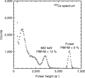
Fig. 8.19
137Cs spectrum with a PbI2 photodetector coupled to LSO scintillator at room temperature
In order to testify the temperature effects on the dark current, experiment is performed and the result is shown in Fig. 8.20. From the figure, one can notice that the variation of dark current is almost linear. For 75 °C the leakage current is only about 10 pA. For flat panel imager, the magnitude of the dark current generated in the photoconductor is an important determinant of medical imaging performance [57]. However, at room temperature, the leakage current is only about 1.8 pA, which is a good number for a radiation detector for medical imaging.
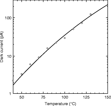
Fig. 8.20
Temperature-dependent leakage current in PbI2 photodetector
The TFT array (dpiX®, 5 × 5 cm2 area) used in the measurements have 127-μm pixel size in a 768 × 768 format. PbI2 powder (5N) is mixed with a proper binder (PIB). The viscosity of the slurry (ink) is adjusted to control the resistivity and the flow through the screen mesh. The screen-printed PbI2 film over the TFT array is shown in Fig. 8.21. Vacuum-deposited palladium (Pd) film is deposited over the PbI2 film leaving 1 cm area from the edges of the PIB film for local ohmic contact. Finally, Pd wires 2 mm diameter is attached to the vacuum-deposited metal (Pd) film for global connections.
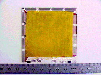
Fig. 8.21
Picture of a TFT array with lead iodide PIB film (screen printed)
Figure 8.22 shows the schematic diagram of the pixel circuit of the TFT array and the storage capacitor with PbI2 film deposited on the active surface of the array. Bias voltage is applied on the film, and the electrical characterization of the film is performed. Table 8.4 presents comparative data of PbI2 films with that of a single crystal.
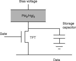
Fig. 8.22
The schematic diagram of the pixel circuit with TFT and storage capacitor
Table 8.4
Comparison of lead iodide properties
Material | Grain size (microns) | Density (g/cm3) | Resistivity (Ω-cm) | μτ product (cm2/V) |
|---|---|---|---|---|
Vacuum-deposited PbI2 | 10–30 | 4.5–5.8 | 2–8 × 10¹² | 1–2 × 10⁻⁶ |
Screen-printed PbI2 | 25 | 5.2 | 5 × 10¹² | 5–8 × 10⁻⁷ |
Single crystal PbI2 | >10,000 | 6.3 | 5 × 10¹³ | 1 × 10⁻⁵ |
Figure 8.23 shows the image of a lead phantom resolution pattern imaged by ~300-μm-thick PbI2 photoconductor on a 127-m pixel. The line pair resolution pattern is obtained with a XDDI TFT array, (768 x 768 pixel arrays, with 127 μm pitch, procured from dpiX, corporation, USA) coated with lead iodide (PbI2) film is shown in (Fig. 8.21) coated with lead iodide (PbI2) film. Fluoroscopic exposure conditions are 60 kVp with 0.1 mm added copper filtration, and exposure rate is 15 frames per second and bias on the photoconductor is 15 V (0.14 V/μm). Figure 8.23 shows that the PbI2 detector can resolve 3.7 line pair per mm almost nearly equal to Nyquist frequency limit of the 127-μm pixel size [58].
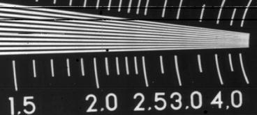
Fig. 8.23
Image of a resolution target taken with a PbI2 array
X-ray detection characteristics of the screen-printed films are also evaluated by irradiating them with exposure from an X-ray tube. A comparison of the X-ray response of the screen-printed and vacuum-sublimed films (of same thickness, 0.13 mm; area, 28 mm2) under identical exposure conditions is shown on Table 8.5. As seen from the table, the response of the vacuum-deposited film is higher by a factor of two, which is mostly due to its higher charge transport parameters. However, the preliminary results for screen-printed films are impressive considering the fact that no special attention was paid to material purity.
Table 8.5
Properties of TlBr detector in comparison to other semiconductor detectors
Material | Atomic number | Density (g/cm3) | Band gap (eV) | E pair (eV) | Resistivity (25 °C) Ω-cm | μτ (e) product cm2/V | μτ (h) product cm2/V |
|---|---|---|---|---|---|---|---|
Si | 14 | 2.33 | 1.12 | 3.62 | Up to 104 | >1 | ~1 |
Ge | 32 | 5.33 | 0.67 | 2.96 | 50 | >1 | >1 |
GaAs | 31, 33 | 5.32 | 1.43 | 4.2 | 107 | 8 × 10⁻⁵ | 4 × 10⁻⁶ |
CZT | 48, 30, 52 | 6 | 1.5–2.2 | ~5.0 | >1010 | 3 × 10⁻³ | 10−5 |
CdTe | 48, 52 | 6.2 | 1.44 | 4.43 | 109 | 3 × 10⁻³ | 2 × 10⁻⁴ |
PbI2 | 82, 53 | 6.2 | 2.32 | 4.9 | 1012 | 8 × 10⁻⁶ | |
HgI2 | 80, 53 | 6.4 | 2.13 | 4.2 | 1013 | 10−4 | 4 × 10⁻⁵ |
TlBr | 81, 35 | 7.56 | 2.68 | 6.5 | >1010 | 10−3 | 4 × 10⁻⁵ |
In summary, our preliminary investigation indicates that the screen-printing method is a very promising technique to fabricate thick X-ray-sensitive layers of lead iodide, which can be applied to medical imaging. The potential of easy scale-up to larger sizes is also evident.
8.4.2 Mercuric Iodide (HgI2)
Mercuric iodide (HgI2) is a layer structure halide of heavy metal. The red variety α-phase is of interest for electronic and nuclear medicine applications. Because of its high density (6.28 g/cc) and high effective Z values (~66), it is a useful material for gamma-ray detection, and when it is doped with boron-rich material/s it can be a potential candidate for thermal neutron detector [59]. The dark conductivity in HgI2 is affected by the ionic conductivity, which is due to the movement of iodine vacancies. However, as a room temperature radiation detector, the ionic conductivity is not dominant. Tunneling is not a factor for HgI2 but the bulk-controlled current is determined by the Poole–Frenkel effect (PFE). However, the leakage current is difficult to attribute to the PFE alone. The bulk resistivity is around 3 × 10¹³ Ω-cm considering electron concentration of 2 × 103 cm−3. The dielectric relaxation time for the material at room temperature has been reported about 25 s [60]. Polycrystalline mercuric iodide (HgI2) is a direct detection material superior to selenium (Se). The effective ionization energy W ef, which is a measure of sensitivity, is much lower than selenium (between 4.9 and 5.1 eV compared to 25 eV of Se at 80 kVp).
The electrical properties, the energy resolution, the peak to background (peak to valley) ratio, and the efficiency of HgI2 are dependent on the number of defect centers and trapping and de-trapping effects. These effects are mostly inherent properties of the material, and the present challenges in HgI2 sensor technology are to increase control of the detector fabrication processes and to modify the detector processing strategy. The presence of the extended defects also affects the uniform charge collection efficiency in HgI2 photo-sensors [61].
Figure 8.24 shows temperature dependence of the electron and hole mobilities in mercuric iodide (HgI2) photodetector. Figure 8.24 (a) represents the electron mobility and (b) represents hole mobility, parallel to the c-axis [62]. Both electron and hole mobilities are found to decrease with increasing temperature. Mercuric iodide (HgI2) crystals have layered structure, and the carrier mobilities are dependent on the crystallographic orientation. Experimental observations show that the electron mobility parallel to the c-axis is always greater than the mobility perpendicular to the c-axis [63].
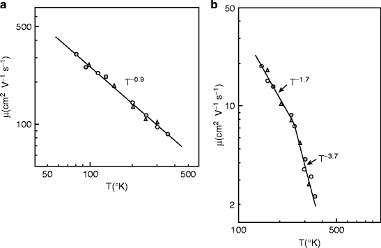
Fig. 8.24
Temperature dependence mobility of (a) electrons and (b) holes (Reproduced with permission from AIP)
The electro-absorption spectrum of HgI2 has been studied by Chester and Coleman [64] as a function of electric field and temperature. Figure 8.25 shows the electro-absorption signal in HgI2 crystal at 300 k for a field of 1.5 × 10⁵ V/cm. From the electro-absorption curve, we can see that the peak occurs around the energy of 2.127 eV, which is less than the band gap energy of the material (2.14 ± 0.005 eV at room temperature). It has been found that when the photon energy exceeds the band gap energy of HgI2, the absorption coefficient is quite large (>105 cm−1) (Fig. 8.25).
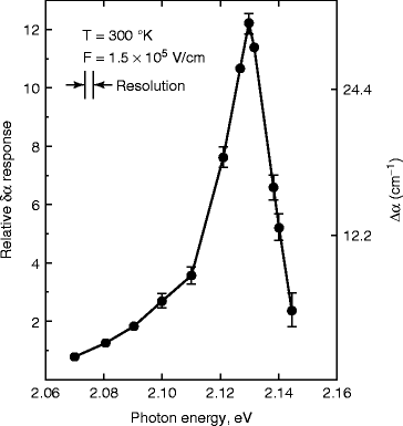
Fig. 8.25
The electro-absorption signal in HgI2 at 300 K (Reproduced with permission from Elsevier Pub.)
Figure 8.26 shows the gamma-ray spectrum of the 662 keV from a 137Cs source taken with a HgI2 detector at room temperature [65]. From the graph, we can find that the resolution is 1.7 % and the peak to valley ratio is 15:1. Experimental observation shows that the crystal has better luminescence property in the band 1 region, which corresponds to near band edge wavelength. Based on these findings, it seems that larger emissions from deeply bound states are indicators of poor detector grade crystals [66].
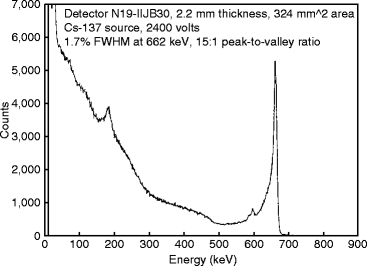
Fig. 8.26
A spectrum of the 662-keV gamma ray from a 137Cs source taken with a HgI2 detector at room temperature (Reproduced with permission from Elsevier Pub.)
In recent years, flat-panel X-ray imagers have been developed with primary application to medical imaging. The technology also is becoming increasingly popular for security screening for its higher specificity. The development of high-sensitivity large-area CT scanners at an affordable cost will be a top priority in medical fields. The most widespread sensors in present flat-panel medical imagers use a phosphor screen coupled with an amorphous silicon photodiode array [67].
Today, the most burning question in medical imaging is to deposit the detector film over a large area of the thin film transistor (TFT) array (active area of the future array is expected to reach 25 × 25 cm2 within the year 2015). It is considered to be the most challenging job since large crystal of HgI2 is difficult to grow. As a result, scientists have paid attention to deposit large-area polycrystalline films either by (1) physical vapor transport (PVT) or (2) screen printing which is also referred to as particle in binder method (PIB) [68]. The challenge with the PVD system is the loss of material, difficulty to make very thick film, and the temperature issue (mercuric iodide changes from alpha phase to beta phase around 127 °C). On the other hand, the second method is capable of making thick film (up to 1 mm) at room temperature and the technology and processing are cost-effective.
As mercuric iodide (HgI2) is an aggressive chemical compound and attacks almost all metals, so a barrier layer has to be applied to cover the metallic local interconnections (an alloy of aluminum with copper and silicon) of the TFT array. The resistivity of the barrier layer should be compatible with the resistivity of the host material, and it should be chemically inert to HgI2. A suitable barrier layer material has been developed, which is inert to the HgI2 and the current conduction through the barrier layer is anisotropic meaning that current conduction is seen only through the perpendicular direction of the flat panel surface. The anisotropic current conduction also minimizes the cross talk between the pixels. Figure 8.27 shows the electronic circuitry with TFT array carrying the HgI2 layer on the top of the barrier layer. The picture underneath is a bare TFT array.
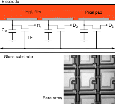
Fig. 8.27
The circuitry of the TFT array with a top HgI2 screen-printed layer over barrier layer. Bottom picture is a bare TFT array
Figure 8.28 shows the picture of mercuric iodide film (red color) over a barrier layer (gray color on the background) deposited on a TFT array (ND-10, 6087-10E®) by screen-printing technology. The active area is ~10 × 10 cm with a 768 × 768 pixel format and 127 pitch. The edges show the aluminum–Si–Cu alloy interconnects for global connections. The bottom picture is a 5 × 5 cm TFT array (dpiX®) covered screen-printed film of HgI2 over a barrier layer. The thickness of the HgI2 layer at different places over TFT array is shown in the Fig. 8.29. The aluminum alloy interconnections are covered with photoresist (edges of the TFT array) to protect the local alloy contacts during the deposition of PIB HgI2 film.
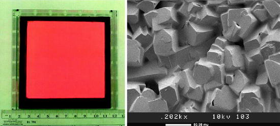
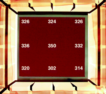
Fig. 8.28
Picture of a screen-printed HgI2 layer (red) over a barrier layer (gray) and the picture on the right hand side shows the scanning electron micrograph (SEM) of the same film (mercuric iodide)
Fig. 8.29
The picture of a 5 × 5 cm TFT array covered with HgI2 over the barrier layer
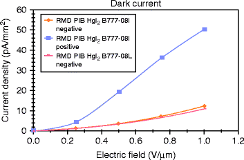
The dark current of a detector is one of the most significant parameters of an X-ray imager. Dark current causes excess charge accumulation in a pixel during the exposure time. If the dark current is constant, it can be subtracted from the signal, but if it is too high then it diminishes the available dynamic range and becomes a source of noise. The noise is proportional to the square root of the dark current.
Figure 8.30 shows the typical dark current under conditions of temporal stability at fields 0.2–1.0 V/μm. The dark current is found to increase with increasing field for both the devices (B777-08L and 08I). The positive biased device shows a larger dark current at room temperature compared to negative biased devices. For negative bias the dark current for 1.0 V/μm applied field is almost the same for B777-08I and 08L devices, and it is approximately 10 pA/mm2, which is a good number of the device for digital mammography application.
 Instrumentation and Its Applications in Nuclear Medicine
 Device Fabrication (Scintillators/Radiation Detectors)
 Theoretical Approach of Crystal and Film Growths of Materials Used in Medical Imaging System
 Medical Imaging
 Basic Principles of Radiation Detectors
 Radiation Exposure: Consequences, Detection, and Measurements


Related posts:
Instrumentation and Its Applications in Nuclear Medicine
Device Fabrication (Scintillators/Radiation Detectors)
Theoretical Approach of Crystal and Film Growths of Materials Used in Medical Imaging System
Medical Imaging
Radiation Exposure: Consequences, Detection, and Measurements
Stay updated, free articles. Join our Telegram channel
Full access? Get Clinical Tree