(1)
Radiation Monitoring Devices Research Nuclear Medicine, Water town, Massachusetts, USA
7.1 Introduction
7.2 Compound Halides
7.2.1 Alkali Halides
7.2.2 Sodium Iodide (NaI)
7.2.3 Cesium Iodide (CsI)
7.3.1 Lead Iodide (PbI2)
7.3.2 Mercuric Iodide (HgI2)
7.3.3 Thallium Bromide (TlBr)
7.6.2 CdTe Crystals
7.8.1 Diamond
7.8.2 Silicon (Si)
7.8.3 Germanium
Abstract
The use of scintillators to detect radiation is a century old, and the discovery and the quest for new inorganic/organic scintillators are ongoing processes. The discovery of thallium-doped sodium iodide (NaI) followed by the earlier discovery of cadmium tungstate (CdWO4) brought revolution in the luminescent physics. In a burst of exploration during the following few years, the scintillation properties of most pure and activated alkali halide crystals were investigated between 1940 and 1950 [1, 2]. Lithium-containing compounds to detect neutrons and the core valance barium fluorides (BaF2) were discovered almost in the same decade. The search for new inorganic and organic scintillators is going on unabated. Indeed, the past two decades have witnessed a variable renaissance in research and development of new scintillator materials prompted in large part by the need for scintillators for precision calorimetry in high-energy physics and for high light output scintillators for medical imaging, geophysical exploration, nonproliferation and national security applications, and numerous other scientific and industrial applications [3–9].
7.1 Introduction
The use of scintillators to detect radiation is a century old, and the discovery and the quest for new inorganic/organic scintillators are ongoing processes. The discovery of thallium-doped sodium iodide (NaI) followed by the earlier discovery of cadmium tungstate (CdWO4) brought revolution in the luminescent physics. In a burst of exploration during the following few years, the scintillation properties of most pure and activated alkali halide crystals were investigated between 1940 and 1950 [1, 2]. Lithium-containing compounds to detect neutrons and the core valance barium fluorides (BaF2) were discovered almost in the same decade. The search for new inorganic and organic scintillators is going on unabated. Indeed, the past two decades have witnessed a variable renaissance in research and development of new scintillator materials prompted in large part by the need for scintillators for precision calorimetry in high-energy physics and for high light output scintillators for medical imaging, geophysical exploration, nonproliferation and national security applications, and numerous other scientific and industrial applications [3–9].
The science and art of fabrication of these highly efficient scintillators are fascinating, and the engineering to build a radiation detector is a part and parcel of medical science, high-energy physics, and exploration geophysics. After the disaster of 9/11, these scintillators (radiation detectors) are also used in commercial sectors to reduce nuclear threats. Most national security applications are concerned with the detection of gamma rays, with energies in the range approximately 10 keV to 10 MeV, and neutrons arising from fissile materials. Modern detector systems consist of three steps: careful selection of materials, device fabrication either from single crystal or from polycrystalline films, and instrumentation. Therefore, we have devoted this chapter on the physics, chemistry, and engineering on the growths of single crystals and polycrystalline films to fabricate most efficient detectors. The instrumentation and the measurements will be dealt with in a separate chapter. The following chart shown in Fig. 7.1 is the chronology of the development of the materials to fabricate the scintillators or radiation detectors.
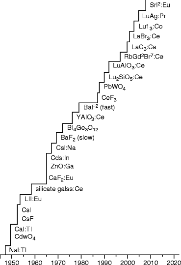
Fig. 7.1
Chronology of the discovery of inorganic scintillators
7.2 Compound Halides
7.2.1 Alkali Halides
Alkali halides (Li, Na, K, Rb, and Cs) are the family of ionic compounds with simple chemical formula XY, where X is the alkali metal and Y is the halogen (F, Cl, Br, and I). The internal crystalline structure at room temperature is center cubic usually face centered (fcc). The advantage of the cubic structured materials is that the internal reflection is less. As a result, these materials show high light output (which is one of the most desirable for a scintillator) compared to hexagonal or orthorhombic or monoclinic. Table 7.1 shows some of the alkali halide compounds. In 1940, with the development of photomultiplier tube (PMT), Hofstadter first developed thallium-activated sodium iodide (NaI) scintillator [1]. In a burst of exploration during 1950s, lithium-containing compounds showed many prospects as neutron detector. As these materials were identified, the procedure to purify and to fabricate detectors either in the form of single crystal or polycrystalline thin films became a routine work. As a result, several procedures were invented or discovered to make single crystals or polycrystalline films from these materials.
Table 7.1
Alkali halide compounds
Halides | Alkali metals | ||||
|---|---|---|---|---|---|
Fluorine | LiF | NaF | KF | RbF | CsF |
Chlorine | LiCl | NaCl | KCl | RbCl | CsCl |
Bromine | LiBr | NaBr | KBr | RbBr | CsBr |
Iodine | LiI | NaI | KI | RbI | CsI |
7.2.2 Sodium Iodide (NaI)
Sodium iodide (NaI) is one of the oldest members of the optical engineering family and is considered by many scientists as a standard optical device in the field of detection technology. In 1950, the discovery of thallium-activated sodium iodide attracted the attention of many investigators who thought that it will be used as a tool in modern scintillation spectroscopy of gamma (γ) rays. It is worth mentioning that in spite of four decades of research, NaI remains as a preeminent scintillator in the field of spectroscopy and nuclear medicine. The most remarkable property of thallium-activated NaI is its remarkable light yield.
Crystal Growth
As the melting point of NaI is low (~650 °C), the single crystal of NaI can be grown easily and inexpensively from the melt in an ambient of nitrogen. Large crystals of NaI single crystal have been grown by directional solidification of the material. A graphite mold is loaded with sodium iodide (NaI) with thallium (Tl) powder in appropriate proportion and heated at 700 °C, and the molten mass is cooled slowly from the bottom in air. On cooling, NaI:Tl solidified and formed a single crystal out of the molten mass.
Large crystals of thallium-doped (0.001 mol fraction) NaI has also been grown by Bridgman–Stockbarger (BS) method. However, press–forged recrystallization of NaI(Tl) crystal under heat and pressure has been reported to produce similar quality crystals as produced by BS method. The main disadvantage of NaI:Tl crystals is that they are very hygroscopic in nature and mechanically not very strong. Thallium-doped (Tl) sodium iodide (NaI) crystals are normally encapsulated in aluminum housings with a wall density of 170 mg/cm2 and an end cap density of 117 mg/cm2.
Figure 7.2 shows the picture of a NaI:Tl single crystal grown by BS method. In order to verify the structure of the single crystal, X-ray diffraction pattern was performed at Massachusetts Institute of Technology (MIT), Cambridge, MA, in a Rigaku X-ray diffractometer model Rotaflex RTP 500 with copper kα radiation. Table 7.2 shows some of the physical properties of NaI.
Fig. 7.2
Picture of a single crystal of tellurium-doped sodium iodide
Table 7.2
Characteristics of thallium-activated NaI
Material | NaI |
|---|---|
Density | 3.67 |
Hygroscopic | Strong |
Emission wavelength (nm) | 415 |
Refractive index | 1.85 |
Primary decay time (ns) | 250 |
Light yield (photons/MeV) | 38 × 103 |
Melting point (°C) | 651 |
Light yield (photons/MeV) | 40,000 |
Structure | bcc |
Thallium-activated sodium iodide crystals are susceptible to radiation damage and are not rugged. Recently, the single crystal ingots of thallium-activated NaI are recrystallized under heat and pressure. The resulting material is a polycrystalline material (Polyscin®) with randomly oriented crystal grains. But surprisingly, the polycrystalline thallium-activated NaI retains its optical character but with improved mechanical strength.
7.2.3 Cesium Iodide (CsI)
Cesium iodide (CsI) is another member of the alkali halide family with many desirable properties (with high atomic number, high density, fast response, and high radiation resistance). It has gained substantial popularity as a scintillating material and is available commercially either doped with sodium (Na) or thallium (Tl). Cesium iodide (CsI) has high resistance to thermal and mechanical shock due to absence of cleavage plane. The emission spectrum is very well matched to the sensitivity characteristics of silicon PIN diode. The luminosity of thallium-activated cesium iodide CsI:Tl can be as high as the theoretical value. Figure 7.3 shows the picture of a CsI:Tl single crystal grown by BS method, and some of the properties of thallium-activated CsI is tabulated bellow in Table 7.3.
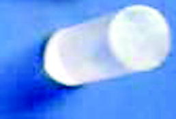
Fig. 7.3
Shows the picture of a single crystal of CsI:Tl grown by BS method
Table 7.3
Properties of cesium iodide scintillator (activator)
Scintillator (activator) | CsI | CsI (Tl) | CsI (Na) |
|---|---|---|---|
Density (g/mL) | 4.51 | 4.51 | 4.51 |
Hygroscopic | Slightly | Slightly | Yes |
Emission wavelength (nm) | 315 | 550 | 420 |
Lower cutoff | 260 | 320 | 300 |
Refractive index | 1.95 | 1.79 | 1.84 |
Primary decay time (μ-s) | 0.016 | 1.0 | 0.63 |
Light yield (photons/MeV) | 2 × 10³ | 54 × 103 | 42 × 103 |
Crystal structure | Cubic | Cubic | Cubic |
The thallium (Tl)-activated cesium iodide (CsI) crystals are being frequently used in medical imaging system (e.g., gamma-ray imaging, X-ray CT, digital radiography, mammography, dentistry, fluoroscopy). The material has high stopping power and good energy resolution [10–12].
Crystal Growth
Typically cesium iodide (CsI) and thallium with 99.99 % purity are used for growing single crystal. Bridgman–Stockbarger (BS) method is very popular for growing single crystal of CsI:Tl. The weight percent of thallium within the matrix is maintained approximately about 0.1 mol% [13, 14]. The charge material is loaded in a quartz ampoule inside a glove box and vacuum encapsulated after degassing. The powder is then melted inside the quartz ampoule, and the quenched solid undergoes through zone refining for a couple of times. The refined material is reloaded in a quartz ampoule inside a glove box and inserted in a BS furnace. The vacuum-sealed quartz ampoule with the charge material is pulled slowly (~0.1–0.5 mm/h) through the furnace with a temperature gradient of 10°/cm. Inside the furnace, argon gas at 2 atm is introduced throughout the entire time of the crystal growth.
Vacuum-Deposited Film: Electronic Portal Imaging Devices
Vacuum–Deposited Film: Electronic portal imaging devices are developed as a digital X-ray imaging system because of the inherent difficulties associated with film-based image capturing system. In order to cover a 25 cm × 25 cm flat-panel imaging arrays with CsI:Tl material, a hot-wall deposition method had been followed at radiation monitoring devices (RMD). The high-vacuum hot-wall epitaxial growth system was capable of depositing future 40 cm × 40 cm flat panel. The process was capable of depositing micro-columnar structure of CsI:Tl (Fig. 7.4).
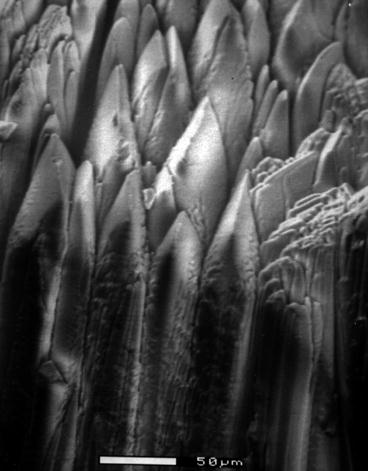
Fig. 7.4
Shows the scanning electron microscopic photograph of a columnar film of thallium-activated cesium iodide deposited by hot-wall epitaxy (Courtesy RMD Inc.)
The CsI:Tl micro-columnar structures as shown in Fig. 7.4 are high-density fibers of CsI:Tl scintillator with a structure resulting from the hot-wall epitaxial growth on a specially designed substrate[15, 16].
X-Ray diffraction pattern of the hot-wall epitaxially grown film of cesium iodide (CsI) doped with thallium (Tl) is performed at MIT, Cambridge, MA, in a Rigaku X-ray diffractometer (model Rotaflex RTP 500) with copper kα radiation. Intensity in arbitrary units is plotted against 2θ value and is shown in Fig. 7.5.
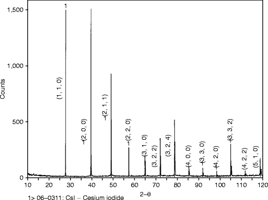
Fig. 7.5
Shows X-ray diffraction pattern of a hot-wall epitaxially grown CsI:Tl film
7.3 Halides of Heavy Metals
These halides of heavy metals like lead iodide (PbI2) [17], mercuric iodide (HgI2) [18], and thallium bromide (TlBr) [19] have high atomic number (Z) together with their density lead to excellent detection efficiency. As for example, the attenuation coefficient of PbI2 is ten times higher at some energies than that of germanium (Ge). Due to their high stopping power, these compound semiconductor crystals of modest thickness will achieve a full energy peak detection efficiency that is equivalent to that of a substantially thicker high-purity germanium (HPGe). The advantages of high band gap for mercuric iodide (2.1 eV) and lead iodide (2.3 eV) have made operation of these devices at room temperatures, and their operations as direct solid-state detector avoid the use of cumbersome scintillator–photomultiplier combinations. As a result, several methods to fabricate the devices either from single crystals or from polycrystalline films have been identified. These methods are challenging in the sense of cost effectiveness and their viability as radiation detectors for use in nuclear medicine.
7.3.1 Lead Iodide (PbI2)
Increasing interest has been focused on layered semiconductor materials like PbI2 and HgI2. These materials have been used for medical imaging and as high-energy resolution room temperature X-ray and gamma (γ) detectors. Their high density and high atomic number allow one to manufacture small, compact detectors with very good volume efficiency ratio [20]. PbI2 as a photodetector shows low leakage current and high quantum efficiency (>60 %) in 350–500 nm region [21]. Table 7.4 shows some of the properties of PbI2.
Table 7.4
Properties of lead iodide (PbI2)
Property | Value |
|---|---|
Band gap | 2.3 eV |
Crystal structure | Hexagonal |
Melting point | 408 °C |
Vapor pressure at 200 °C | 10−5 torr |
Dielectric constant | 21 |
Density | 6.2 g/mL |
Resistivity (ρ) | >1013 Ω-cm |
Electron/hole product (μτ) | 10−5/ 2 × 10⁻⁶ cm2/V |
Crystal Growth
Single-phase PbI2 polycrystalline material is first synthesized directly from pure lead (Pb) and iodine (I) in a stoichiometric ratio with excess of Pb by two-temperature vapor transport method (VTM). The polycrystalline material is then purified through zone refining. The purified material is loaded in a vertical Bridgman apparatus and single crystal of PbI2 has been grown [22–24]. During the growth of the crystal, the maximum temperature of the hot zone in the furnace is maintained at ~450 °C, and the temperature gradient (dT/dx) is maintained at 5°/cm rate. Following these parameters, the growth rate of PbI2 single crystal is typically around 10 mm/h. The grown single crystal shows resistivity typically between 1010 and 1011 Ω-cm [25, 26]. Figure 7.6 shows the picture of a vapor-phase-grown single crystal of lead iodide (PbI2).
Fig. 7.6
The picture of a vapor-phase-grown single crystal of lead iodide (PbI2) (Reproduced with permission, SPIE)
Vacuum-Deposited Film
Vacuum evaporation is another method of depositing polycrystalline PbI2 films. During resistive vacuum evaporation, almost 70–80 % of the source material is lost on the walls of the chamber. We designed a hot-wall resistive vacuum evaporation and have been able to recover almost 50–60 % of the lost material inside the vacuum chamber. The three-dimensional sketch below shows the relation of the deposition rate of PbI2 with wall and source temperatures (Fig. 7.7).
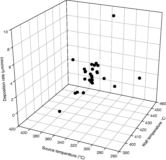
Fig. 7.7
Shows the relation of the deposition rate of PbI2 with wall and source temperatures
X-ray diffraction of the hot-wall epitaxially grown lead iodide (PbI2) film is performed at MIT, in a Rigaku X-ray diffractometer (model Rotaflex RTP 500) with copper kα radiation. Intensity in arbitrary units is plotted against 2θ value and is shown in Fig. 7.8.
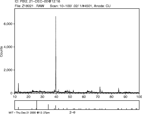
Fig. 7.8
XRD pattern for hot-wall PbI2-deposited film (film # 151HWPbI2 # 6)
Screen-Printed Film
Extensive research in recent years has shown that the flat-panel X-ray image detectors based on a large-area thin-film transistor (TFT) or switching diode scanned active matrix array (AMA) is the most promising digital radiographic technique and suitable to replace the conventional X-ray film/screen cassettes for diagnostic medical digital X-ray imaging applications (mammography, chest radiography, and fluoroscopy) [27, 28]. Recent development in the flat-panel imaging matrix is expected to produce commercial large area of panels that can extend an area of 40 cm × 40 cm. To cover such a large area is not possible by small single crystal or vacuum-evaporated film. In order to cope with the technical difficulty, research organizations have come up with screen-printed films. The technology is old and the method of screen printing goes back to early 1960 [29].
The lead iodide (PbI2) slurry (bright yellow in color) is prepared by mixing PbI2 powder with a proper binder. The slurry thus prepared is used for screen printing on a previously cleaned ITO-coated glass substrates. After printing, the films are subjected to air drying for 30 min before sintering them in an oven. Figure 7.9 shows a PbI2 film deposited on an ITO glass.
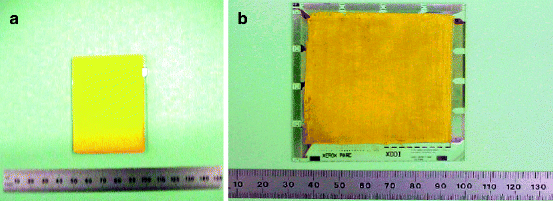
Fig. 7.9
(a) Screen printed PbI2 film deposited on an ITO glass. (b) TFT array covered with screen-printed PbI2 film
Following deposition of the PbI2 films on ITO glass, large-area lead iodide films are deposited over the TFT array (Fig. 7.9b), and extensive characterization of the physical and electrical properties has been carried out. The bulk film density had also been estimated by measuring the film dimensions and its weight. In addition, evaluation of the surface morphology and grain size has been conducted using scanning electron microscopy (SEM). Film morphology gives an idea about the grain boundaries and defects that can be scattering centers for charge carriers. Figure 7.10a and b shows the scanning electron micrograph of the vacuum-deposited and the screen-printed films, respectively. The pictures show that PbI2 is a layered structure with alternate Pb and I2. The particle sizes for vacuum-deposited film vary between 0.25 and 1 μm, while the grain sizes of the screen-printed film are larger and vary between 0.75 and 2.5 μm.
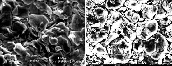
Fig. 7.10
Scanning electron micrograph of PbI2 films. (a) Vacuum-deposited film, (b) screen-printed film
7.3.2 Mercuric Iodide (HgI2)
Mercuric iodide (HgI2) due to its high atomic number (Hg-80, I-53), large band gap (2.15 eV), and required low energy (W eff) to create electron hole pair has been a subject of interest for medical imaging. It has been studied for the past 50 years owing to its efficiency as a nuclear spectrometer at room temperature [30, 31]. The potential of HgI2 nuclear detector technologies will certainly be more fully realized as more progress is made toward the understanding of the material properties responsible for wide variability in detector performance [32].
Figure 7.11 shows the picture of a single crystal of HgI2. In HgI2 configuration, each mercury (Hg) atom is tetrahedrally bonded to four-iodine (I2) atoms in a covalent bond. These tetrahedral bondings are stacked in the z-direction, resulting in weak I–I bonds. Using calculated values for electronic band structure and optical matrix elements, one can model the absorption coefficient as a function of the incident photon energy [33].
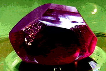
Fig. 7.11
Shows a single crystal of mercuric iodide (HgI2) (Photo courtesy: Constellation Technology, Florida)
Room temperature operation combined with a high resolution and good energy resolution opens the way to miniaturization and portability of the detectors and spectrometers [34]. The polymeric form of HgI2 can reside in two phases, red α phase, which is stable but transforms into yellow orthorhombic β phase above 127 °C. However, the orange α-phase tetragonal structure of HgI2 has much attention as a potential candidate for medical imaging and synchrotron applications. The layered structure of HgI2 exhibits a pronounced anisotropy of thermal and mechanical properties.
Figure 7.12 shows the alpha-phase crystal structure of mercuric iodide. The polymeric forms of HgI2 are known as red α-HgI2 and yellow β-HgI2 [35]. The tetragonal HgI2 is stable up to ~127 °C, and at higher temperatures, it transforms into yellow orthorhombic β-HgI2, which exhibits a tendency to be present in a metastable state on the surface of the α-HgI2.
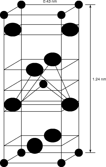
Fig. 7.12
Shows the elemental cell of tetragonal alpha-phase (α) mercuric iodide (HgI2) mercury  iodine
iodine Growth of Single Crystal of Mercuric Iodide (HgI2)
Successful growth of high-quality α-HgI2 single crystals is largely dependent upon the purity of the starting material. The repeated sublimation procedure is followed by sealing the quartz ampoule inside a Bridgman furnace with a temperature gradient along the length of the furnace tube. The technique of the crystal growth can be described as physical vapor transport (PVT) technique.
The initial starting material (reagent grade HgI2) is first purified by sublimation process which is repeated for three to four times. The material thus obtained is undergone zone refining for further purification. Single crystal of HgI2 is obtained by applying vapor-phase methodology.
Thermodynamic calculations of the vapor-phase stoichiometric composition of HgI2 in a closed system (when the temperature inside is maintained ~200 °C) show that in equilibrium condition, the vapor phase contains only HgI2 [36, 37].
Figure 7.13 shows the schematic of a crystal growth furnace of mercuric iodide (HgI2). It has been reported that the furnace is capable of growing single crystal of HgI2 up to 1,000 g in weight [38].
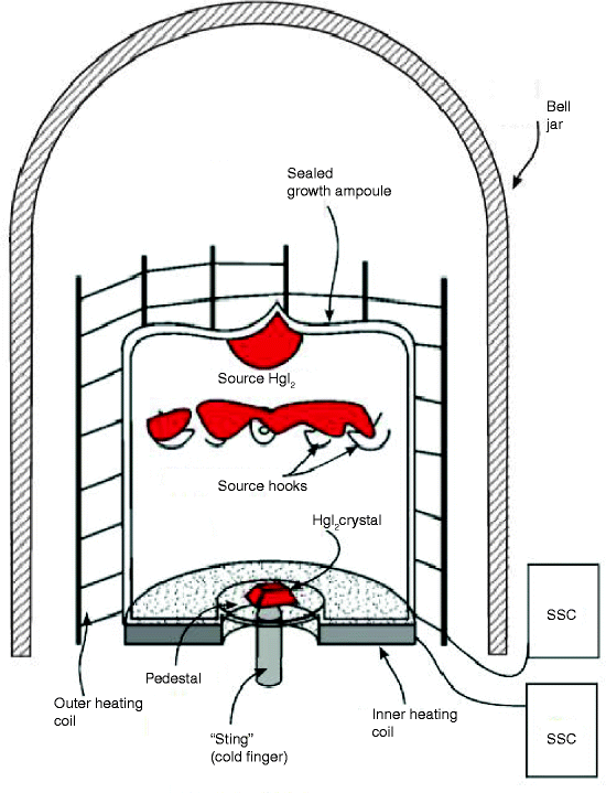
Fig. 7.13
Shows the schematic of a crystal growth furnace of mercuric iodide (HgI2)
An alternative method for direct synthesis of HgI2 has been reported by Pencotka and Kaldis [39] which has been carried at a temperature exceeding 300 °C in a stream of a carrier gas saturated with the vapors of mercury and iodine. However, precipitation from aqueous solutions by reactions of potassium or sodium iodide (KI or NaI) with mercury chloride (HgCl2) or nitrate ((HgNO3)2) seems to be simpler, but the product after reactions shows the presence of nitrate or chloride.
Vapor-phase-grown mercuric iodide (HgI2) single crystal has been reported by Ponpon et al. [40]. The material is synthesized by reaction of the constituent elements with excess of iodine. The synthesis is followed by double stage purification (zone refining under reduced pressure). The growth method is controlled by vapor condensation of the purified charge. After natural seeding during heating and condensation, the crystal grown over the seed is pulled slowly at 1–10 mm/day (Fig. 7.14).
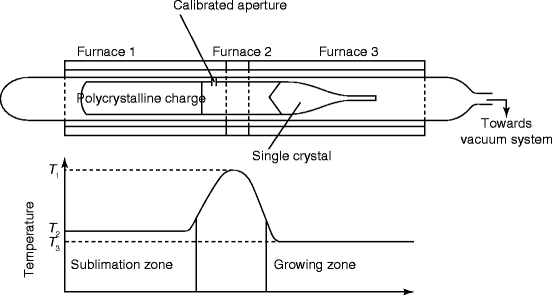
Fig. 7.14
Shows the schematic of a vapor phase growing HgI2 single crystal
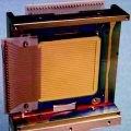
Screen-Printing System
In mid-2001, Siemens Medical System offered a 41 × 41 cm2 detection area electronic portal devices (EPIDs), following the commercial 30 × 40 cm2 detection area EPIDs of Varian medical system [41]. To deposit ~133 mg cm−2 over such a large area with uniform thickness and stoichiometry is difficult, challenging, and expensive, especially some materials which change their phase at a higher temperature. A more cost-effective and easy way of covering such a large area is by adopting screen-printing technology—an old and matured technology [29]. We are going to present a very promising scintillating material (HgI2), which has shown much promise [42]. Indeed, with its high atomic number, mass density, and relatively high detection efficiencies at diagnostic energies, screen-printed thick film (300–500) of HgI2 is comparable to other potential scintillating materials that are being used in commercial radiation detectors [43, 44].
The Technology for HgI2 Deposition
Figure 7.15 shows the schematic and the photograph of an HgI2 screen-printing system. The system uses HgI2 particle in binder, where the particles of pure HgI2 powder are mixed with a binder prepared from a proper polymer dissolved in a solvent. The viscosity of the binder is controlled so that the slurry/ink can easily pass through the screen mesh. At the same time, the resistivity of the binder becomes compatible with the resistivity of HgI2, to facilitate the flow of X-ray-induced charge across the boundaries between the HgI2 grains and the binder. To prevent the corrosion of the local aluminum alloy connecting lines, a barrier layer is deposited over TFT arrays, before HgI2 deposition. The barrier layer allows anisotropic current flow (only in perpendicular direction of the flat panel) and minimizes the cross talk between the pixels.
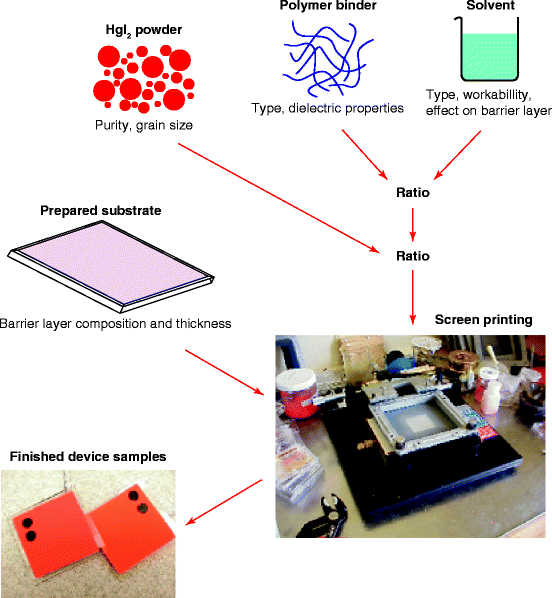
Fig. 7.15
Shows the schematic and the photograph of the screen-printing system of HgI2
7.3.3 Thallium Bromide (TlBr)
The average atomic mass of thallium (Tl) is comparable with that of lead (Pb) and mercury (Hg). Therefore, it will not be unrealistic to place TlBr in the halides of heavy metals. TlBr crystals have the CsCl-type simple cubic structure with density of 7.56 g/cm3. The compound melts congruently at 480 °C and, therefore, is well suited for melt-based growth methods such as Bridgman and Czochralski processes. Table 7.5 shows some of the properties of thallium bromide (TlBr).
Table 7.5
Properties of thallium bromide
Molecular weight | 284.31 |
Melting temperature | 460 °C |
Crystal structure | Cubic, CsCl-type structure |
Density | 7.453 g/mL |
Transmission range | 0.44–40 μ |
Hardness | 11.9 mhos |
Solubility in water | 0.05 g/100 g |
Cleavage planes | No cleavage |
Band gap energy | ~2.7 eV |
Resistivity | 1012 Ω-cm |
Growth of Single Crystal of Thallium Bromide (TlBr)
Thallium bromide (TlBr) is dense and has high atomic number with wide band gap and has potential as an efficient and compact room temperature nuclear radiation detector [45]. Pixelated thallium bromide (TlBr) detectors have been successfully used in gamma-ray (γ-ray) spectroscopy and medical imaging [46].
Single crystal of TlBr is grown by Bridgman–Stockbarger (BS) method in vertical two-zone furnace [47]. Distilled and zone-refined high-purity, ultradry TlBr was placed in an evacuated quartz ampoule and moved through a two-zone furnace very slowly. Typical growth rates for BS process are 1–10 mm/h; however, certain layered structures require slower rates. The temperature of the upper zone is kept at about 600 °C while that of the lower zone is kept at 400 °C, which acts as an annealing temperature for the grown crystal. The dropping rate of the ampoule determines how close the conditions at the solid–liquid interface come to equilibrium. At very slow rates, the system operates close to equilibrium, which is desirable for growth of defect-free crystals. Figure 7.16 shows a 26.5-cm (in length) single crystal of TlBr grown by BS method. Experimental observations show that lead (Pb) and indium (In) impurities degrade the electrical and optical properties of TlBr crystal [48]. There are some reports of growing single crystal of TlBr by electrodynamic gradient process (EDG) [49].
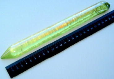
Fig. 7.16
Shows a 26.5-cm (in length) single crystal of TlBr grown by BS method
7.4 Lanthanide Halides
In the beginning of the twentieth century, lanthanum halide scintillators are attracting much attention of the scientific community in nuclear spectroscopy, because of their almost ideal scintillation properties, like optimal energy resolution (<3 % at 662 keV), excellent time resolution (~300 ps), and good efficiency [50–52]. The crystals are available commercially from Saint-Gobain Crystals under the brand name BrilLianCeTM. These scintillators have high light yield, fast response, and good energy resolution [53, 54]. The single crystal of lanthanum halides can be grown as big as 1,000 mL in volumes. Recent survey shows that the lanthanide crystals are more attractive than high-purity (HP) germanium (HPGe) for gamma-ray (γ-ray) measurements. These detectors are commonly used in nuclear and high-energy physics research, medical imaging, diffraction, nondestructive testing, nuclear treaty verification and safeguards, and geological exploration [55, 56].
7.4.1 Cerium-Activated Lanthanum Chloride (LaCl3:Ce)
Lanthanum chloride crystals have hexagonal structure, and its density is ~3.9 g/cm3. The melting point of the material is ~860 °C and can be grown by two-zone Bridgman–Stockbarger process [57, 58]. Lanthanum chloride (Lacl3, mp ~848 °C) and cerium chloride (CeCl3, mp ~849 °C) (10 mol%) after drying under argon atmosphere are loaded inside a quartz ampoule and is sealed under vacuum. The lower and the upper temperatures are maintained at 450 and 960 °C, respectively, with a temperature gradient (dT/dx ≈ 4°/cm). The boule is pulled very slowly (1.5 cm/h). Typical growth rate in BS method is approximately 5–10 mm/h. Figure 7.17 shows the picture of a LaCl3 single crystal grown by Bridgman–Stockbarger (BS) technique. The impurities are seen to have segregated at the bottom and top of the crystal. Further purification of the crystal is done by zone refining in an argon atmosphere. Table 7.6 shows some of the properties of lanthanum chloride (LaCl3).
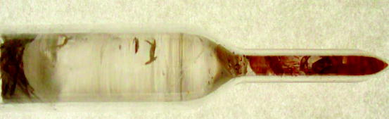
Fig. 7.17
Picture of a single crystal of LaCl3 grown by Bridgman–Stockbarger method
Table 7.6
Properties of lanthanum bromide (LaCl3)
Crystal structure | Hexagonal |
|---|---|
Density (g/mL) | 3.89 |
Hygroscopic | Yes |
Effective Z | 37 |
Index of refraction | 1.90 |
Light yield (photons/MeV) | 49,000 |
Peak wavelength (nm) | 350 |
Principal decay time (ns) | 25 |
Attenuation length (cm) | 2.8 |
Energy resolution | 3.2 |
Melting temperature (°C) | 862 |
7.4.2 Cerium-Activated Lanthanum Bromide (LaBr3:Ce)
The material LaBr3 is supposed to be superior to CsI and NaI in quality like light output, as well as high proportionality [52]. Single crystal of LaBr3 activated with cerium (Ce3+) is grown by Bridgman method. LaBr3 and CeBr3 powders (99.99 %) are loaded in quartz ampoules and are sealed in an inert atmosphere [59]. The ampoule is passed slowly (0.5 mm/h) through a two-zone furnace. The upper zone of the furnace is kept at a temperature of 850 °C, which is higher than the melting point of LaBr3 (783 °C). The lower zone of the furnace is kept ~680 °C. The growth rate of crystal is observed approximately 0.5 mm/h when the temperature gradient inside the furnace is kept around 28 °C/cm. The orientation of the growth of the crystal is seen to depend on the rate of the movement of the ampoule inside the furnace [60]. Figure 7.18 shows a single crystal of LaBr3 grown by Bridgman–Stockbarger (BS) method in our laboratory. Table 7.7 shows some of the properties of lanthanum bromide (LaBr3).
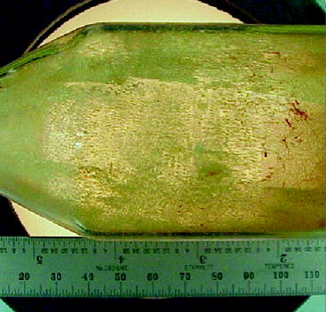
Fig. 7.18
Picture of a LaBr3 single crystal grown by BS method (Courtesy: RMD)
Table 7.7
Properties of lanthanum bromide (LaBr3)
Crystal structure | Hexagonal |
|---|---|
Density (g/mL) | 5.3 |
Hygroscopic | Yes |
Effective Z | 46.9 |
Index of refraction | 1.88 |
Light yield (photons/MeV) | 80,000 |
Peak wavelength (nm) | 380
Related posts: Instrumentation and Its Applications in Nuclear Medicine Instrumentation and Its Applications in Nuclear Medicine
 Theoretical Approach of Crystal and Film Growths of Materials Used in Medical Imaging System Theoretical Approach of Crystal and Film Growths of Materials Used in Medical Imaging System
 Medical Imaging Medical Imaging
 Characterization of Radiation Detectors (Scintillators) Used in Nuclear Medicine Characterization of Radiation Detectors (Scintillators) Used in Nuclear Medicine
 Radiation Exposure: Consequences, Detection, and Measurements Radiation Exposure: Consequences, Detection, and Measurements
Stay updated, free articles. Join our Telegram channel
Full access? Get Clinical Tree
 Get Clinical Tree app for offline access

|