(1)
Radiation Monitoring Devices Research Nuclear Medicine, Water town, Massachusetts, USA
3.1 Introduction
3.3 Polarization
3.4 Electrode Design
3.6 Coplanar Design
3.7 Pixelated Design
3.11.1 Shot Noise
3.11.2 Flicker Noise
3.11.3 Burst Noise
3.13 Dead Time
Abstract
Mathematical modeling has been used routinely in the design and analysis of semiconductor radiation detectors because it saves development time in the initial stages and saves the manufacturing cost as a whole. Moreover, one can easily change parameters, such as trapping and de-trapping times (τ t, τ D), electric field strengths (ε), electron–hole mobility (μ n, μ h), and electrode designs, during computer simulation and can minimize the polarization and maximize overall detection efficiency (η) of the detector without spending much time in the laboratory. Thus, during computer simulation, these parameters are changed partially or fully until the model spectrum matches closely to the real spectrum [1, 2].
3.1 Introduction
Mathematical modeling has been used routinely in the design and analysis of semiconductor radiation detectors because it saves development time in the initial stages and saves the manufacturing cost as a whole. Moreover, one can easily change parameters, such as trapping and de-trapping times (τ t, τ D), electric field strengths (ε), electron–hole mobility (μ n, μ h), and electrode designs, during computer simulation and can minimize the polarization and maximize overall detection efficiency (η) of the detector without spending much time in the laboratory. Thus, during computer simulation, these parameters are changed partially or fully until the model spectrum matches closely to the real spectrum [1, 2].
The numerical simulation as described above is of great interest during the analysis, design, and modeling of a radiation detector. Recently an accurate model for determining the three-dimensional (3-D) distribution of charge pulses produced in a semiconductor detector has been developed [3, 4]. The simulation presents a significant reduction in computational timing and has become a fruitful tool for 3-D configuration. The model also takes account of different parameters of the detector, for example, the pulse processing, the charge collection efficiency, and the associated electronic noise [5]. However, choosing parameters in a system is a challenge, especially in the network design. As for example, to reduce the statistical noise to an acceptable level and to accurately correlate with experimental work require heavy computational maneuvering due to the large number of photons and their history [6].
The next key question for mathematical modeling is the choice of algorithm, which directly impacts key parameters in a system. For example, a simple threshold-based detection algorithm may consider data from each sensor and therefore requires no communication. However, simulations are necessary to understand the behavior of a system, the characteristics and limitations of the algorithms, and the impacts on the system from changes in parameters. It requires thorough knowledge of the radiation detector and the related physics involving the source of generation of X-ray, the interaction of the X-ray beam with the detector and finally the imaging process. The Monte Carlo method is the most regularly used numerical simulation adopted to address the interaction problem of X-rays with the scintillators.
Experimental observations show that the efficiency of charge collection in the detector was influenced by the ratio of charge collection and trapping and de-trapping times of the charge carriers, and one should make sure that simulations should have taken into account these factors. In principle, the findings from the simulations depend on the parameters of the deep levels; hence, it is important to work with parametric quantities representing the conditions present in state of the art of the detectors. However, using a model with one mid-gap level, one can simulate both acceptors and donors in a simpler way than the deep-level model [6]. However, Petasecca et al. have adopted a model, which includes radiation-induced deep level recombination centers, and the study of Shockley–Read–Hall (SRH) statistics has been successful to evaluate the radiation damage effects in p-type silicon [7].
Simulation has been used for a long time for modeling the medical imaging on a domain composed of an electrode surrounded by its eight neighbors in a 3-D geometry. During simulation, the charge induction efficiency is computed assuming standard electron lifetime (τ) and mobility (μ). The bi-parametric spectrum and pulse height spectra are then simulated, taking into account a realistic noise model. The pulse height and rise time standard deviations are then computed using spectral density analysis of the detector. In case of pixelation geometry, numerical simulation has been able to optimize energy resolution of a medical imager with wide pixel and small interpixel spacing [8].
3.2 Trapping and De-trapping
In an imaging detector, charge trapping and de-trapping effects appear in many compounds (CdTe, CdZnTe, HgI2, PbI2, PbF2, CsI, etc.) and elemental semiconductors (Si and Ge) used in radiation (imaging) detector [9]. As a matter of fact, polarization effect [10] is believed to be the possible cause of trapping and de-trapping of carriers including change of defect structure of the detector. The trapping and de-trapping of carriers will change the space charge distribution in the radiation detector and will modify the induced charge due to radiation.
In presence of traps, the electric field within the detector becomes weaker with time and shows polarization, which ultimately decreases the counting rate with time. But in absence of traps, the current density (J) of an insulator (semiconductor with high resistivity at room temperature) will follow the relation of Mott and Gurney [11] and can be presented mathematically as
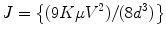
(3.1)
In the presence of traps, the above equation will transform into an exponential equation as follows:
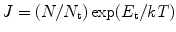
where N is the number of total charges produced due to external radiation, N t is the number of trapping centers at energy level E t, k is Boltzmann constant, and T is the absolute temperature. When E t is very large (several eVs), the space charge limited current does not induce significant conductivity and consequently does not increase the noise level.
(3.2)
The charge carriers (N) under the influence of the bias voltage will decrease in the presence of traps, and the number of the charge carriers that will be trapped will depend upon the number of traps and the energy level of the trapping centers. As a result, the number of free charge carriers will decrease and can be expressed mathematically as
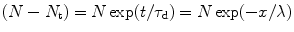
where τ d is the mean drift time, x is the distance traveled by the carriers (x = v d t), λ is the mean free path, and v d is the drift velocity. Now if the carriers are reemitted due to thermal process, the probability of such process will give rise to a value reciprocal to the de-trapping time as
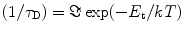
where τ D is the de-trapping time, E t is the energy level of the trapping center, and ℑ is the frequency factor.
(3.3)
(3.4)
When periodicity of a perfect single crystal is perturbed due to the presence of foreign materials or crystal defects, discrete energy levels (E t) are introduced into the band gap that represent some defect centers or trapping centers. These defect centers are also called generation–recombination (G-R) centers. These recombination centers can act as traps, where a carrier can be captured and subsequently be injected back into the band. Although not contributing directly to recombination, trapping and de-trapping can impact heavily on the overall carrier dynamics and can affect the detector performance. In absence of traps, the induced charge due to the external radiation is a function of the interaction location (x) and can be defined as
![$$ = q{N_0}\left[ {({v_{\mathrm{ h}}}{\tau_{\mathrm{ h}}})/(d)\{ (1 - \exp [( - x/{v_{\mathrm{ h}}}{\tau_{\mathrm{ h}}})\} ] + [({v_{\mathrm{ e}}}{\tau_{\mathrm{ e}}})/d\{ (1 - \exp [( - x/{v_{\mathrm{ e}}}{\tau_{\mathrm{ e}}})\} } \right] $$](/wp-content/uploads/2017/03/A308734_1_En_3_Chapter_Equ00035.gif)
(3.5)
However, in the presence of traps, the lifetime (τ) of the carriers will be modified to τ h = (1/N t v th σh) and τ e = (1/N t v th σ e), where τ h, and τ e are the hole and electron lifetimes, N t is the number of trapping centers at an energy level E T, v th is the thermal velocity of the carriers, and σ h and σ e are capture cross sections of the holes and electrons. Now the time-dependent current I(t) due to trapping and de-trapping can be written as

and I(t) = 0 when t ≥ τ r, where τ r is the transit time of the carrier.
(3.6)
Following Hecht formula the above Eq. 3.6 can be written as
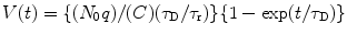
where C is the preamplifier (Fig. 3.1) capacitance. If the de-trapping time is not negligible, the voltage pulse will show fast and slow components with time and the above Eq. 3.7 will be modified to:
![$$ \mathrm{ For}\;\mathrm{ fast}\;\mathrm{ component}:\;V(t) = \left[ {\{ ({N_0}q)/(C)\} \{ {\tau_{\mathrm{ e}}}/{\tau_{\mathrm{ r}}}\} ][\{ (1/{\tau_{\mathrm{ D}}} + {\tau_{\mathrm{ e}}}/{\tau_{\mathrm{ d}}})\} \{ 1 - \exp (t/{\tau_{\mathrm{ e}}})\} } \right] $$](/wp-content/uploads/2017/03/A308734_1_En_3_Chapter_Equ00038.gif)
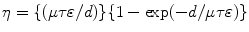
where τ e = {(τ d τ D)/(τ d + τ D)}. For slow component, however, it is difficult to reach a satisfactory analytical solution. If the charges are generated near to one of the electrodes and surface recombination is neglected, the efficiency (η) of the detector will be given by
(3.7)
(3.8)
(3.9)
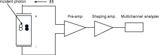
Fig. 3.1
Schematic diagram of detector and the associated electronics
When surface recombination is considered to be present, the above equation will transform into

where s v is the surface recombination velocity, μ is the mobility, τ is the lifetime of the carriers, and ε is the electric field.
(3.10)
The surface recombination velocity (s v) is defined as the number of carriers recombining per second per unit area divided by the excess concentration over the equilibrium value at the surface. It is a function of density and energy of interface states, capture probabilities, carrier concentrations, and degree of occupancy of the interface states and can be defined mathematically as

where N ts is the density of surface states per unit area, σ is the capture cross section, and v th is the thermal velocity of the carriers. Surface recombination velocity (s v) plays an important role in determining the mobility-lifetime (μτ) product—the quality factor of the radiation detector. Surface recombination is a special case of recombination, which is analyzed in terms of surface recombination velocity (SRV) instead of lifetimes (τ h and τ e). The X-ray spectra and photocurrent methods are able to give a rough estimate of mobility-lifetime product (μτ), by analyzing either the charge collection efficiency as a function of the applied electric field or the shape of the X-ray photo peak [12].
(3.11)
Frequently mobility-lifetime products for electrons and holes are measured rather than separately determined. For a given detector geometry and field strength, the mobility-lifetime products determine the charge collection efficiency and are often quoted when evaluating nuclear detector materials [13].
At a semiconductor surface there are surface energy states with energies within the energy gap of semiconductor. These energy states can be divided into layer states (owing to the characteristics of the oxide layer; they arise from the absorbed ions, molecules, or imperfections). The interface states owing to the characteristics of the semiconductor-oxide interface arise from initial semiconductor surface treatment before oxide formation, and their behavior is similar to the bulk recombination centers.
It has been reported that the self-trapped hole in cesium iodide (CsI) crystal consists of two bound iodine (I) atoms (the Vk center, I2 −) aligned along <100> axis of the body-centered cubic (bcc) lattice. However, in alkali halide crystals the situation is quite different. Here one can find two-atom Vk centers. On the other hand, in lead fluoride crystal (PbF2), the hole can be shifted to one of the 12 nearest neighbor lead (Pb) atoms by displacement of two fluorine (F) atoms between them [14].
The band gaps of certain materials like diamond and mercuric iodide (HgI2) are large, and these materials show high resistivity. As a result, the neutrality of the crystal after the passage of ionizing radiation is not restored in the time interval between two events. Therefore, one can expect space charge accumulation within the crystal. These charges might be trapped partially for a period of time depending on the position of the trapping levels introduced in the forbidden gap. These immobile trapped charges will constitute an electric field opposite to the direction of the applied field. Thus, the field distribution due to the external field will no longer remain constant. The modified field in presence of the traps can be expressed mathematically as
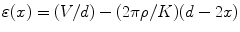
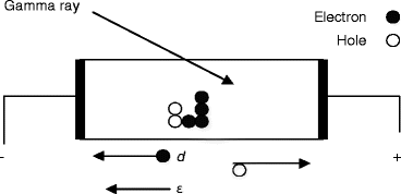
where ρ is the space charge per unit volume and is equal to (N 0 E 0 q/ϵv), N 0 is the number of radiations counted by the crystal, q is the electronic charge, E 0 is the energy of the incoming radiation of volume υ, V is the applied bias voltage, K (K = ϵ/ϵ 0, where ϵ is the permittivity of the material and ϵ 0 is the permittivity in vacuum and is equal to 8.85 × 10⁻¹² F/m) is dielectric constant of the material, and d is the distance between the electrodes. Figure 3.1 represents a schematic of a radiation detector with associated electronics, and Fig. 3.2 shows the physical activities inside the detector once it is irradiated by the incoming radiation.
(3.12)
Fig. 3.2
Schematic of a basic planar detector where charge carriers are created by external radiation and separated by an external bias. d is the distance between electrodes, and ε is the electric field
3.3 Polarization
Polarization is defined as the time-dependent performance of the detector. Possible causes of polarization include trapping, de-trapping, and change of defect structure in the detector. The trapping and de-trapping of charge carrier change the space charge distribution in the detector and thus modify the electric field profile. The charge collection efficiency will be altered correspondingly through the change in the average drift length of the carrier, as we have already noticed from the relation established in Eq. 3.10.
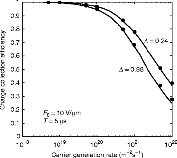
Figure 3.3 shows the photo-generated charge rate vs. total charges collected when recombination due to trapping and de-trapping is taken into consideration. The upper curve represents the total charges for mammographic application, and the lower one represents for radiographic applications [15]. Apart from the trapping and de-trapping, the effectiveness of moving charge carriers away from surface recombination centers can also affect the image resolution of the detector as we can see from the relation
![$$ \eta = \left[ {\{ 1/(1 + s/\mu \varepsilon )\cdot (\tau \varepsilon \mu /d)\} \{ 1 - \exp ( - d/\mu \tau \varepsilon )\} } \right] $$](/wp-content/uploads/2017/03/A308734_1_En_3_Chapter_Equ000313.gif)
where s is the surface recombination velocity. It has been pointed out by Levi et al. [16] that whenever charge carriers are generated near the surface (electrode), surface recombination in addition to the bulk trapping will change the Hecht equation.
(3.13)
Fig. 3.3
Monte Carlo simulation of charge collection efficiency vs. carrier generation rate when trapping and de-trapping are taken into considerations. F 0 is the electric field, Δ is the absorption depth, and T is the exposure time (Reproduced with permission: IEEE , [115] and Elsevier Pub.)
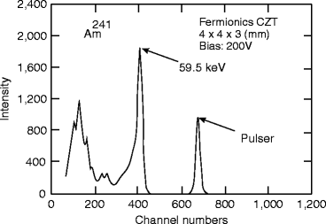
Semiconductor like cadmium zinc telluride CdZnTe (CZT) has poor charge collection efficiency because of their large amount of trapping centers. As a result, peaks in a spectrum have broad shoulder to the lower energy side, a typical sign of high hole trapping [17, 18]. Figure 3.4 shows the 57Co spectrum for a CZT detector.
As a result, FWHM value for the particular peak is difficult to measure, and we can use Hecht equation to take into account all these trapping centers. Accordingly, Eq. 3.13 will be modified to
![$$ {\eta = (Q/{Q_0}) = [({\lambda_{\mathrm{ e}}}/d) 1 - \exp (- d- x)/{\lambda_{\mathrm{ e}}}][\{({\lambda_{\mathrm{ h}}}/d)\}1 - \exp ( - d - x)/{\lambda_{\mathrm{ h}}})}$$](/wp-content/uploads/2017/03/A308734_1_En_3_Chapter_Equ000314.gif)
where x is the distance from interaction site to cathode, d is the thickness of the detector, λ is the mean free path, and e and h in the subscripts denote electron and hole. The value of λ e is almost 200 times larger than λ h, so the trapping incidents have to account for λ h only. In this case, the induced charge due to energy deposition of X-ray (or γ-ray) is equal to the initial charge multiplied by η. The parameters λ e and λ h are determined by comparing the shape of the peaks (tails) in response functions with the ones in measured X-ray or gamma-ray spectra.
(3.14)
The trapping and de-trapping times may vary considerably among different traps, so we can expect the time-dependent detector performance with different time scale. The polarization may have drastically different effects on the X-ray spectra. The difference in time scale may be related to the fabrication procedures of the detector, the impurities and defects that are introduced during single crystal growth, and the behavior of the contacts due to different deposition techniques. Other factors that contribute to the polarization are the incident radiation energy, flux, penetration depth, and detector impurities.
Gradual change in energy resolution, count rate, or peak position over time is addressed as the consequence of polarization. In mercuric iodide (HgI2), polarization is generally thought to be the effect of the degradation of the exposed material in the air, and it is suggested by many that immediate encapsulation of the material after processing can prevent the degradation. Another type of polarization is observed in p-n junction diodes and also in HgI2, which is due to the formation of dead layer. It causes a gradual reduction in X-ray peak counts or peak position over a period of several hours after application of bias voltage. The dead layer thickness measured in HgI2 detectors varies from 0.91 μm at 5.89 eV to 1.6 μm at 22.16 keV [19]. According to some experts, the cause of these phenomena is due to the electrodrift and diffusion of impurities [20] or space charge formation [21].
Dead layer is formed due to the formation of surface channels. Surface channels on the other hand actually appeared due to the formation of surface states during the surface preparation of the material (device). The surface channels actually control the I–V characteristics of the diode and become a source of noise (leakage current) in the detector. It has been suggested that purification of the material, improvements of the growth process, increasing bias voltage, lowering flux, and/or increasing operating temperature and use of thin device have greatly reduced the polarization effects [22, 23]. Most of the time, the thicker device shows polarization effect the most due to the inherent properties of the bulk material.
Sometimes, a pronounced tail is observed in the high-energy side of the spectrum when HgI2 is used in gamma-ray spectrometer. However, continuous bias application reduced the effect very much. The possible explanation of this is the formation of charge multiplication process associated with Auger recombination. The process involves charge trapping of electron and recombination of holes. As a result, energy released by the recombination is transferred to a remaining trapped electron, which is ultimately ejected to the conduction band [24].
In cadmium telluride (CdTe) and cadmium zinc telluride (CdZnTe), polarization effect is believed to be due to the trapping of electrons that ultimately causes an accumulation of space charge and a reduction of the depletion layer thickness. According to some experts, the chlorine doping to increase the bulk resistivity may be one of the causes of polarization in these materials. However, careful processing, proper purification, and use of proper contact material and electrode design can minimize the polarization effect considerably [25].
3.4 Electrode Design
Let us consider the metal contact over a semiconductor material. When a metal is brought into intimate contact with a semiconductor, the Fermi level of the metal is fixed in relation to the bands of the semiconductor. It has been observed that in most of the semiconductors, the Fermi level at the interface comes about one-third the band gap (E g) above the valence band [26, 27]. When there is no metal in contact with the semiconductor, the Fermi energy level at the surface is qϕ 0. Assuming an acceptor surface state density D s and equating the charge induced on the metal surface to the surface state charge and the space charge in the semiconductor, we can write the barrier height ϕ B as

where ![$$ a = \left\{ {\left. {{\varepsilon_{\mathrm{ i}}}/({\varepsilon_{\mathrm{ i}}} + \delta {q^2}{D_{\mathrm{ s}}})} \right\}} \right., b = \left[ { - a\chi + \{ \left( {1 - a} \right)({E_{\mathrm{ g}}}/q - {\varphi_0})\} } \right] $$](/wp-content/uploads/2017/03/A308734_1_En_3_Chapter_IEq00031.gif) , δ is the interfacial layer, χ is the electron affinity of the semiconductor, ϕ m is the metal work function, and ε i is the dielectric constant of the interfacial layer. The values of ϕ 0 and D s can be expressed as
, δ is the interfacial layer, χ is the electron affinity of the semiconductor, ϕ m is the metal work function, and ε i is the dielectric constant of the interfacial layer. The values of ϕ 0 and D s can be expressed as

(3.15)
, δ is the interfacial layer, χ is the electron affinity of the semiconductor, ϕ m is the metal work function, and ε i is the dielectric constant of the interfacial layer. The values of ϕ 0 and D s can be expressed as(3.16)
When the number of the surface states is high, ϕ B = (E g/q − ϕ 0), and the barrier height is independent of the metal work function φ m. On the other hand when the surface states is small and ϕ B = (ϕ m − χ), the metal work function plays an important role.
The estimation of barrier height is important in the sense that it determines the current flow. The current density (J) can be expressed mathematically following Richardson thermionic emission as
![$$ J = A{T^2}\exp ( - q{\phi_{\mathrm{ B}}}/kT)[\exp (qV/kT) - 1] $$](/wp-content/uploads/2017/03/A308734_1_En_3_Chapter_Equ000317.gif)
where A is the Richardson constant for thermoionic emission, k is Boltzmann constant, T is temperature in absolute, q is the electronic charge, and V is the applied bias voltage. The barrier height can also be determined from the width of the space charge region. For abrupt p-n junction, the depleted width is
![$$ W = {{[2\varepsilon ({V_{\mathrm{ bi}}} - V - kT/q)/(q{N_{\mathrm{ D}}})]}^{1/2 }} $$](/wp-content/uploads/2017/03/A308734_1_En_3_Chapter_Equ000318.gif)
where V bi is the built-in voltage, N D is the donor concentration density, and ε is the dielectric constant of the material.
(3.17)
(3.18)
Electronic states at the surface of semiconductor detectors that are produced during the final surface treatment and by adsorbed vapors during the operation of the device lead to the formation of surface channels. The thickness of the surface channels is of the order of Debye length or bulk screening length (L D), which is several tenths of a millimeter in good detectors. The L D can be expressed mathematically as
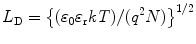
(3.19)
The surface channel changes the electric field inside the detector and its surface in such a way that there are some regions where the electric field is much higher than an average electric field. It has been shown experimentally that the surface channels are the cause of dead layer [28, 29]. The better side of the detector is therefore the n-side for n-type surface channel and p-side for the p-type surface channel. An n-type surface channel leads to a dead layer beginning at the p-contact.
In coaxial Ge (Li) detector, the (1/r) dependence of the electric field may partly compensate the effect of the channel on the surface of the electric field. With usual contact arrangement (n-contact at the outside and p-contact in the core), a p-channel in a conventional coaxial detector can lead to a lower surface electric field than a planar one. This leads to a near perfect I–V characteristic with coaxial detectors compared to a planar one. An n-type channel in a coaxial detector makes the surface electric field near the core even larger, thus leading to a poor reverse characteristic.
The metal electrodes are used to impose an electric field across the semiconductor and collect the charge created by the incident radiation. In principle these electrodes should be ohmic, meaning that the current–voltage relation through these contacts should be linear. As the current produced by the applied bias is always larger than it is created by the incident radiation, blocking contacts are generally applied in Si and Ge devices. Whereas in mercuric iodide (HgI2) and cadmium telluride (CdTe) where the band gap of the materials is high, the ohmic contacts are desirable to get a lower leakage current. However, deposited metal electrodes appear to produce Schottky barrier-like contacts that can limit the charge collection efficiency for at least one type of carrier. As a result, contact metal became a subject of research in the fabrication of room temperature nuclear detectors.
The choice of a metal surface barrier for semiconductor radiation detector is in practice made on the basis of a reverse current characteristic. Metals with work functions greater than 4.4 eV are all acceptable. Evaporated gold (Au) adheres poorly to Ge surface. On the other hand, chromium (Cr) adheres well to Ge surface but brittle and easily cracked by external pressure. Platinum (Pt) adheres well but requires high temperature to melt the metal and needs electron beam evaporation. Of all the metals tried so far for ohmic contacts, nickel (Ni) and palladium (Pd) both give acceptable small reverse currents, and the metals adhere well to the surface. In addition to that, these metals can be evaporated from a tungsten filament.
In high-purity germanium (HPGe), two types of contacts are formed. For n+ type, lithium (Li) of several millimeter thick is diffused at 270–300 °C, and for p-type contact, boron (B) is implanted inside HPGe. When HPGe is p type, lithium (Li) diffusion forms a p-n junction, leaving a 1-mm undepleted Ge region that reduces the low-energy detection sensitivity. However, in coaxial HPGe detector, Li will not diffuse significantly into the crystal at low temperature. A phosphorus implantation, however, is an alternative procedure, which requires a careful post-implant annealing.
For mercuric iodide (HgI2), palladium (Pd) and carbon (C) are usually used as contact materials for X-ray and gamma-ray detectors. Sputtered Pd, however, introduces undesirable surface states. The dark current technique has been used to measure the barrier height, which gives rise to a value of about 1.2 eV for both Pd and C contacts. In case of cadmium telluride (CdTe), electroless deposition of gold (Au) and platinum (Pt) has been found to be very successful [30]. During chlorine reaction (to increase the bulk resistivity), cadmium (Cd) leaves the material to the solution as Cd+ and tellurium (Te−) precipitate on CdTe surface as p-type film mainly at the interface. Part of the Te is found to exist in the deposited layer of Au or Pt, allowing the contaminated contact metal to react with Te. This does not happen with Cd. However, the reaction kinetics of Au and Pt with Te is different. In the presence of oxygen, the Te layer can form TeO x layer, which is a semiconductor material, and the metal complex forms a hetero-junction between TeO x and CdTe with highly distributed interfacial regions [31]. In case of tunneling, it can be distributed to Au or Pt or Cl− (doped).
Diffused indium (In) forms a low resistive good contact to n-type CdTe crystal at 300 °C and for n-type CdTe material. In a neutral argon (Ar) atmosphere, it forms a good has been successfully used in good X-ray and alpha (α)-particle detectors. The surface of CdTe is etched or polished, and a layer of indium (In) or the oxide of indium (InO3) is deposited. It is then thermally diffused within the temperature limits, and a p-type contact is made with gold (Au). However, for gamma-ray detector, metal–semiconductor–metal (M-S-M) structure with Au or Pt contacts is very popular.
In lithium-drifted (Si–Li) silicon, sputtered-coated amorphous silicon (α-Si) has been used as n-type contact. For p-type contact, boron is being implanted on the silicon surface, and both of these contacts have been successfully used in silicon radiation detector [32].
p- and n-type contacts in cadmium zinc telluride (CZT, Cd0.96Zn0.04 Te) are formed by diffusing gold (Au) and indium (In). However, chlorine is doped in the crystal to (i) increase the bulk resistivity and (ii) to compensate background impurities and defects. Due to the low leakage currents (<10 nA at room temperature), CZT detectors are usually fabricated with platinum (Pt) and gold (Au) ohmic contacts by using metal–semiconductor–metal (MSM) structures. CZT detectors with Pt contact have shown good energy resolution of 1.4 % (FWHM) at 59.5 keV (at –37 °C) [33]. However, poor hole charge transport has resulted in long tail spectra. On the other hand, p-i-n structures in CZT detectors that are used in gamma-ray detectors are formed by p- and n-type contacts. These contacts are formed by liquid phase epitaxial deposition (LPD) of p- and n-type crystals of HgCdTe.
3.5 Frisch Grid Design
It has been reported that the Frisch grid design can deliver better sensitivity to a radiation detector over planar design [34, 35]. The prototype parallelepiped design with side grids is limited to thin dimensions due to weighting potential restrictions. The design allows one to fabricate relatively large volume detectors with reduced contamination in the measurement region. Moreover, the device utilizes several physical effects to increase gamma-ray interaction efficiency and energy resolution including geometrical weighting, small pixel, and Frisch grid effects [36].
Figure 3.5 shows the schematics of a planar device and a Frisch grid device. The Frisch grid design and its performance indicate that trapezoid prism (TP) design is a better choice over parallelepiped design because the γ-ray interaction (F i) is better in the interaction region. As a result, TP design gives rise to higher sensitivity and higher rejection ratio [37], which can be understood from the following relation:
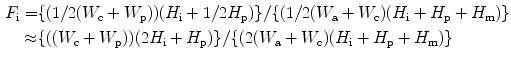
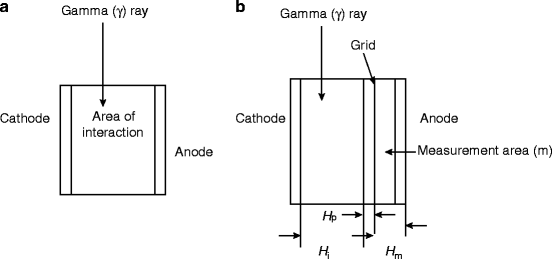
where W c and W a are the width of the cathode and anode, respectively; W p is width at the previous region center; H i is the height of the interaction region; H p is the height of the previous region; and H m is the measurement region height. Figure 3.6 below shows the schematic of the general features for a geometrically weighted semiconductor Frisch grid radiation spectrometer.
(3.20)
Fig. 3.5
Schematic of (a) planar device and (b) Frisch grid device
Fig. 3.6
Schematic of the general features for a geometrically weighted semiconductor Frisch grid radiation spectrometer (Reproduced with permission, Elsevier Pub.)
The probability of distribution of the normalized γ-ray radiation under uniform irradiation can be expressed mathematically as

where H d is the total detector height, x refers to the distance from the anode toward cathode, and θ is the acute angle at the anode (Fig. 3.6). The combined effects of the geometrical weighting and pixilated detector cause the formation of pseudo-peak which enhances the overall resolution of a geometrically weighted semiconductor device. The Frisch grid effect, on the other hand, increases the overall device performance due to the screening of the hole charge carriers’ motion [38].
(3.21)
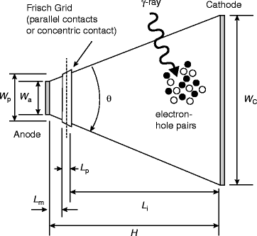
In Frisch grid design, a potential is applied to the device such that electrons are drifted toward the cathode. Placing a grid near the anode ensures that the induced signal forms only from the drifted electrons. Several methods of creating a Frisch grid effect without an embedded grid have been studied [39, 40]. The most effective design so far is the noncontacting Frisch grid detector, where a bar-shaped detector is inserted into a conductive ring, which also allows for an insulator filling between the Frisch ring and the detector body [41]. Figure 3.7 shows the schematic of a bar-shaped Frisch grid detector.
Fig. 3.7
The different parts of a bar-shaped Frisch-grid detector. (a) The inner bar has been detached from the conductive ring. (b) Partial insetion of the bar inside the conducting ring (Reproduced with permission from Elsevier Pub.)
Charge induction on the anode occurs mainly in the gap region (measurement region) between the anode and Frisch ring. The highest energy resolution at 662 keV (1.7 % FWHM) has been reported with Frisch ring edge placed at 2 mm back from the anode [42].
To compensate electron trapping, Luke [43] employed a linear compensation technique using subtraction circuit with relative gain applied between channels, assuming good material uniformity. Recently, He et al. proposed a method [44] for depth correction of electron trapping. In coplanar geometry, fine tuned outer most grids and outer most gaps minimize the difference in weighting potential [45, 46]. Using radial sensing method, energy resolution of 2 and 2.4 % FWHM at 662 keV γ-ray energies has been reported.
It has been observed that coplanar design is very effective and promising to achieve energy resolution, and has provided an important breakthrough to overcome the hole-trapping problem in compound semiconductors. Unfortunately, the design is expensive, and the process is complicated. Furthermore, interstrip leakage current becomes an additional source of noise in the circuit. In order to minimize these effects, a newly designed detector named capacitive grid detector has been proposed by Montemont et al. [47].
In the capacitive Frisch grid design, the bulk detector is insulated with a dielectric layer which enables one to modify the weighting field (E w) without affecting the applied field (E). The weighting field corresponds to an instantaneous variation in charge separation and represents the transit field that follows Gauss equation:

And the dielectric relaxation time constant τ = ε/σ, where σ is the conductivity of the bulk detector material, ε is the dielectric permittivity, and E w is the weighting field. Since the instantaneous current produced by the charge q is conserved, we have div σE = 0.
(3.22)
Figure 3.8 shows the schematic of a capacitively coupled Frisch grid device with operational circuit. The thin insulating layer shown in the above figure is fabricated with a high insulating material like Kapton® or Mylar®, and a metal ring is formed over the insulator.
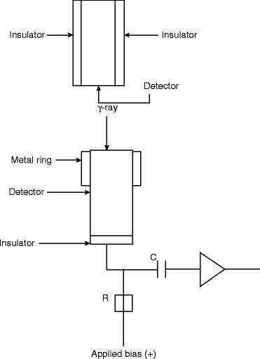
Fig. 3.8
Schematic of a capacitive Frisch grid design with operational connections. R resistor, C capacitor
Figure 3.9 shows pulse height spectrum from a Capacitive Frisch Grid detector using 137Cs source. For comparison a simulated spectrum is shown in the figure.
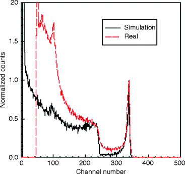
Fig. 3.9
Pulse height spectrum from a capacitive Frisch grid detector using 137Cs source (Courtesy: RMD)
3.6 Coplanar Design
The recent introduction of coplanar grid techniques has led to resurgence in interest in developing large volume compound semiconductor detectors that have a γ-ray response and good spectrographic resolution [48]. As a matter of fact, the coplanar grid technique is essentially an evolution of the classical Frisch grid technique to reduce position-dependent charge collection effects in gas detectors [49]. Compared to simple planar contacted device, a coplanar grid detector has two anode electrodes in the form of interdigital grids. One is called the collecting electrodes, and the other is a non-collecting electrode. The collecting electrode is provided with a bias voltage (V g), whereas the second one is kept at ground potential. Signals are collected from both of the electrodes and subtracted to give a net output signal. In the single-electrode configuration, signal is collected only from one grid, and optimization of detector response is accomplished by adjusting the relative areas of the two grid electrodes (Fig. 3.10).
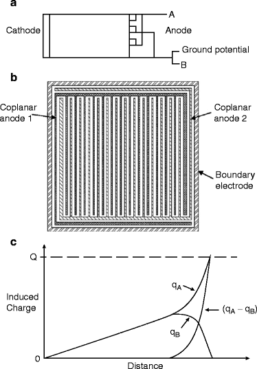
Fig. 3.10
(a) Coplanar grid structure with coplanar electrodes, (b) coplanar grid design with two coplanar anodes and a boundary electrode, and (c) calculated induced charge signal on the anode A and B as a function of the position of the drifting charge –Q originating near the full area cathode. (q A − q B) denotes the external subtraction of the two signals on A and on B electrodes (Courtesy: P.N. Luke)
Both the designs show no dependencies of the output signals on the hole collection. Thus, both the designs effectively eliminate the problem of poor hole transport. However, semiconductor materials also exhibit significant levels of hole trapping. This introduces a depth dependence on the net induced signal since electron trapping is dependent on the depth of the semiconductor surface (here from the grid to cathode region). With single-electrode readout method, one has to design the electrode to match the electron transport characteristics and not the gain adjustments like the conventional coplanar-grid technique.
Hole trapping in semiconductor planar detector inhibits its ability to efficiently collect total charge, because in planar geometry, good energy resolution depends upon efficient charge collection of both polarities. The charge collection in semiconductor radiation devices will follow the same principle as semiconductor devices, and the continuity equations for excess charge carriers (neglecting trapping de-trapping phenomena) can be presented mathematically as

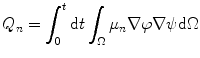
where μ n , D n , and τ n are mobility, diffusion coefficient, and lifetime of the electrons, respectively, and G n is set to an impulse of unit charge. As a result, the charge induced at a selected electrode of the radiation detector can be presented following Ramo’s theory [50] as
where∇ψ is the weighting potential, which we have discussed earlier. For a planar device, we have to consider the contribution due to hole in addition to the contribution due to electrons, and similar model can be set forward.When we solve Eq. 3.24, we can set the photocurrent J ph as
![$$ {J_{\mathrm{ ph}}} = qd[{\mu_n}n(x) + {\mu_p}p(x)]\varepsilon (x) - q{\mu_n}{n_0} + {\mu_p}{p_0})V/d $$](/wp-content/uploads/2017/03/A308734_1_En_3_Chapter_Equ000325.gif)
where q is the electronic charge, d is the thickness of the detector, μ n is the mobility of electrons n(x), μ p is the mobility of hole, p(x)ε(x) is the electric field, and V is the bias voltage. Therefore, the charge collection efficiency (CCE) can be derived from Eq. 3.25 as
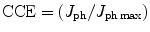
where J ph max is the maximum photocurrent which can be measured assuming no trapping and de-trapping of the photogenerated carriers. However, when the electrode structure is complex, induction efficiencies that have high-frequency spatial components and have large numbers of interaction positions can make the solution complex, leading to prohibitive computing time [51]. In large CZT crystal the nonuniformity around tellurium (Te) is responsible for nonuniformity of electron transport and deterioration of the energy resolution along coplanar detectors [52, 53].
(3.23)
(3.24)
(3.25)
(3.26)
In our previous discussion, we have mentioned that in semiconductor detector, holes are collected in a less efficient way compared to their counter charge electrons. As a result, the planar geometry has been modified in several ways where the detector signal is dependent on the efficient collection of electrons.
The two most effective designs are coplanar and Frisch grid geometry. Both Frisch grid- and coplanar-based designs have proven to be better choice over planar design because of its ability to calculate the energy resolution from the detection of electrons [54, 55]. However, all of the methods suffer from problems, which include leakage current between the anode and grid, processing difficulties, or electric field distortions.
3.7 Pixelated Design
In some semiconductors, single-polarity charge sensing through a coplanar grid electrode is applied to overcome the difficulties encountered due to poor hole transport in the semiconductor detector. Unfortunately, even with single-polarity charge sensing technique and methods to compensate for electron trapping, such as relative gain and depth sensing, the variations in electron trapping and material nonuniformity can still degrade the energy resolution. In pixelated detector (PD), however, the small pixel effects can reduce the effects of hole trapping [56].
Pixelated detectors are operated generally in the charge integrating mode and are dependent on the diffusion of the charge carriers from the point of its origin. These detectors can be approximated by Gaussian distribution function with a standard deviation σ and can be defined as
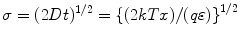
where D is the diffusion coefficient, t is the time, k is Boltzmann constant, T is the temperature, q is the electronic charge, x is the drift distance, and ε is the electric field.
(3.27)
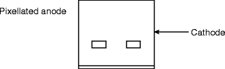
Figure 3.11 shows the schematic of a pixelated detector (PD). In PD, the anode is generally pixelated, and the cathode remains as planar. Using Hecht equation we can write the charge induction efficiency in a pixelated device as
![$$ (Q/{Q_0})=\eta = [\{{{(\mu \tau )}_{\mathrm{ h}}}\varepsilon \} /\{ (d)\}][\{1-\exp(-x/{{(\mu\tau)}_{\mathrm{h}}}\varepsilon \}] + [\{{{(\mu \tau )}_{\mathrm{e}}}\;\varepsilon\}/\{(d)\}]\quad\times[\{1-\exp(x-d)/{{(\mu\tau)}_{\mathrm{e}}}\varepsilon \}].$$](/wp-content/uploads/2017/03/A308734_1_En_3_Chapter_Equ000328.gif)
where μ is the mobility, τ is lifetime of the carriers, ε is the electric field, d is the thickness of the detector, and x is the interaction distance from the cathode.
(3.28)
Fig. 3.11
Schematic of a pixelated detector (PD)
For an event occurring near the cathode (x ≈ 0), the above equation will transform to
![$$ ({Q_{\mathrm{ c}}}/{Q_0}) = [\{ {{(\mu \tau )}_{\mathrm{ e}}}\varepsilon \} /\{ ({d^2})\} ][\{ 1 - \exp ( - d/{{(\mu \tau )}_{\mathrm{ e}}}\varepsilon \} ] $$](/wp-content/uploads/2017/03/A308734_1_En_3_Chapter_Equ000329.gif)
For an event near the anode (x ≈ d), it will convert the Hecht equation as
![$$ ({Q_{\mathrm{ A}}}/{Q_0}) = [\{ {{(\mu \tau )}_{\mathrm{ h}}}\varepsilon \} /\{ (d)\} ][\{ 1 - \exp ( - d/{{(\mu \tau )}_{\mathrm{ h}}}\varepsilon \} ] $$](/wp-content/uploads/2017/03/A308734_1_En_3_Chapter_Equ000330.gif)
Q c represents the charge (channel number on the ADC) induced on the planar cathode, and Q A is the charge induced on one of the pixelated anode, and Q 0 is the total charge induced by the interaction of the radiated source (without any de-trapping or recombination). The value (Q c/Q A) represents the ratio between the peaks (taking into account one pixel at a time), and one can estimate the values (μτ)h, (μτ)e from the equation (Q c/Q A). Recently, the current-mode ADC chip prototype for the readout of depleted field-effect transistor (DEPFET) particle pixel detectors with high spatial resolution has been reported. The measured signal-to-noise ratio (SNR) of the ADC, as reported by Perie et al., is about 660, where the cyclic ADC is based on current-mode memory cell [57]
(3.29)
(3.30)
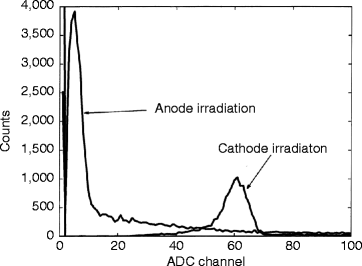
Figure 3.12 shows 141Am spectra from the cathode signal. As the bias is increased, the planar spectra are more prominent because holes can travel further before they are being trapped. But the pixelated anode spectrum is more prominent than the planar spectrum due to the electron movement, which generates all of the induced charge. The induced charge produced near the pixel is dependent on the depth of interaction and the weighting potential. However, a thicker detector should have a weaker dependence on depth compared to a thinner detector, assuming the pitch depth (pixel size) is same in both cases. As a matter of fact, depth-sensing cathode to anode signal (C/A) can be expressed mathematically as
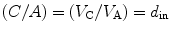
where V C and V A are the voltage signal on the cathode and voltage signal to the anode and d in is the interaction depth. In order to correct for depth interaction, a gain adjustment must be performed. However, the measured signal is seen to vary from voxel to voxel due to weighting potential of the pixelated anode, electron trapping, and nonuniformity of the crystal along the length. However, at higher biases, electron trapping is lowered, and the weighting potential becomes a larger factor in determining the resolution [58].
(3.31)
Fig. 3.12
 Instrumentation and Its Applications in Nuclear Medicine
 Device Fabrication (Scintillators/Radiation Detectors)
 Theoretical Approach of Crystal and Film Growths of Materials Used in Medical Imaging System
 Medical Imaging
 Characterization of Radiation Detectors (Scintillators) Used in Nuclear Medicine
 Radiation Exposure: Consequences, Detection, and Measurements


141Am spectra from the cathode signal (Reproduced with permission, IEEE, Baciak and He)
Related posts:
Instrumentation and Its Applications in Nuclear Medicine
Device Fabrication (Scintillators/Radiation Detectors)
Theoretical Approach of Crystal and Film Growths of Materials Used in Medical Imaging System
Medical Imaging
Characterization of Radiation Detectors (Scintillators) Used in Nuclear Medicine
Radiation Exposure: Consequences, Detection, and Measurements
Stay updated, free articles. Join our Telegram channel
Full access? Get Clinical Tree