Fig. 11.1
Illustration of the PET probe principle
The probe provides events of a different type, where one of the two annihilation photons interacts in the additional detector. The excellent spatial resolution of the probe is indicated in the figure by the smaller size of the detector elements. This type of events, categorized as probe–ring events, will define a thinner line of response and consequently delimit a much smaller volume of possible source positions, resulting in an improved inherent spatial resolution.
The idea of combining events from multiple data sets with different resolutions was suggested first by Clinthorne et al. [5]. Their approach was to boost a standard PET ring with an internal high-resolution ring with limited efficiency. The result of their study was quite surprising: Even a relatively small portion of events with high spatial resolution dramatically improves the imaging performance, especially when small details are sought in the image. The imaging performance was quantified via a version of Cramer–Rao bound [6], a curve that relates resolution and variance (or equivalently, contrast and resolution) of a particular realization of reconstructed image. The bound shows a device-characteristic trade-off between the image resolution and the variance and offers a way to compare two independent systems. The results are quoted as a noise advantage, expressed as the ratio of the standard deviations in images from the two systems, both reconstructed at the same target resolution.
Figure 11.2 shows the noise advantage of a standard PET ring supplemented by a full internal ring providing an additional 13 % of high-resolution events compared to a stand-alone external ring only. The example shown in the figure refers to a disk of a homogeneous activity and resolutions of standard and probe–ring events assumed to be 4 mm FWHM and 1 mm FWHM, respectively.
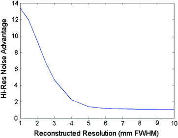
Fig. 11.2
Ratio of image variance for a ring–ring data set versus a data set complemented with 13 % of high-resolution probe–ring data. Simulation assumed a double-ring arrangement, 4-mm FWHM ring, and 1-mm probe resolution
There is little improvement in adding high-resolution data while spatial reconstruction remains above to the system resolution of the external ring. Below that margin, the noise advantage starts to rise, reaching a value of 10 at 2-mm resolution. Since for Poisson governed systems the standard deviation is proportional to the square root of the event count, a ratio of 10 in standard deviations translates into 100 times less events required in a mixed system to reach comparable image quality. The anticipated performance of a probe-equipped system will hence rely on the spatial resolution of collected events.
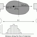
Figure 11.3 shows a probe–ring event with those parameters that are relevant for computing the spatial resolution of such events. The resolution is calculated in the direction perpendicular to the line of response as there is little information on position along the line of response from a single interaction (see also Chap. 3). In that direction the contribution to spatial resolution due to limited resolution of the detector elements will be
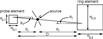

where (see also figure) D is the separation of the sensors, θ 1 and θ 2 are the impact angles, σ D and σ C are resolutions of respective detector elements in circumferential and longitudinal (or in depth) direction, and α measures the relative distance d 1/D of annihilation position along the line of response.
Fig. 11.3
Schematic drawing of the probe and ring detector element and parameters, relevant for computing resolution of probe–ring events
(11.1)
For a perpendicular impact, the expression is simplified to α 2-weighted sum of circumferential resolution of both detectors. The resulting curve is drawn in Fig. 11.4 for three conceivable probe intrinsic resolutions. The variance has a broad minimum, and annihilations as far as 10 cm from the probe can still be resolved with spatial resolution nearly identical to the intrinsic spatial resolution of the probe. The effects of annihilation acolinearity have to be added to the above expression, noting however that its spatial resolution also depends on distance of detectors from the annihilation point:
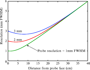
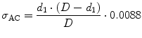
Fig. 11.4
Resolution of the probe–ring event in the direction perpendicular to the line of response. Horizontal axis indicates the distance of the annihilation from the high-resolution detector
(11.2)
For events close to the probe (in its “focus”), this contribution tends to be quite small (0.7 mm at 10 cm) and can be safely ignored compared to the geometrical resolution given in Fig. 11.4.
From the figure, it can be seen that a probe with a 1-mm inherent resolution will be able to resolve annihilation sources with 1-mm spatial resolution, comparable to high-resolution events from the inner ring of the setup suggested by Clinthorne et al., making all their conclusions valid for the PET probe concept as well.
Since probe–ring events will be mostly collected from a single position of the probe, the probe–ring data set will suffer from limited angle anomalies. However, using the basic image of the external ring and adding the probe–ring data set should circumvent appearance of artifacts in the combined image.
A potential clinical application of the PET probe would be detection and localization of a prostate cancer. The prostate is hard to image as it is located in-between significant amounts of obscuring tissue. For a ring geometry of a PET system, this means that the radiopharmaceutical has to be imaged from a relatively large distances, overlying blurring and noise from the obscuring tissue over the region of interest. Since the outcome of the disease is strongly related to its precise localization (extra-prostatic growth, number of focal points), the current image quality is inadequate for proper staging and treatment planning [7]. One way to overcome present misgivings would be to add a probe to the PET ring and place the probe in the vicinity of the prostate. The probe can explore the proximity of the prostate to the rectal cavity, following examples from transrectal ultrasound [8] and endorectal magnetic resonance imaging [9], or can be a strategically placed external probe. In either case, a near 1-mm resolution of PET-amplified probe in the prostate region could be achieved, allowing for an improved localization and staging of the disease.
11.2.1 The Requirements of the Probe and Selection of Probe Composition
One of the most important features of the detector serving as the probe is its excellent spatial resolution. This should be combined with:
An excellent timing resolution for proper event matching
An appropriate energy resolution to be able to recognize events where photons were scattered in the body prior to detection
Sufficient relative transparency to prevent interference with the external ring while intercepting about 10 % of high-resolution data required to maintain image quality
Physical compactness and sturdiness for practicality of use
These requirements are hard to satisfy simultaneously. The present detection materials only match some of the requirements while compromise others. Multiple implementations are possible based on either scintillator-based detectors [10] or solid-state detectors [11], which seem to be a compelling choice with practically infinite spatial resolution [12].
The PET probe implementation presented here falls in this latter category. The selected silicon detectors provide unprecedented spatial resolution, by far exceeding requirements of nuclear medicine. In other aspects, the timing resolution is not perfect, but manageable [13], and its low efficiency/stopping power can be compensated by stacking multiple detector layers. The low stopping power can also be seen as an advantage, since external PET ring data will be only slightly modified by the presence of the probe. With robustness of silicon, the practicality issue is also resolved, adding a bonus of the probe being non-perturbed by operation in a magnetic field [14].
While trying to outline general properties of a PET probe, the following sections nevertheless refer to a specific implementation of the probe, developed within the MADEIRA collaborative project.
11.3 The PET Probe Prototype
The PET probe is essentially an addition to an existing PET ring. Consequentially, most efforts were concentrated on the development of the additional detector, the probe, assuming availability of a suitable external ring. In the following discussions, the probe will be assumed to be interfaced to a standard whole-body human PET scanner like those characterized in [1, 2].
11.3.1 Properties of Silicon Detectors
The silicon detectors are standard tools in particle physics. They are used to track charged particles close to the interaction point. The silicon detectors intended for the PET probe are a slightly modified version of the originals.
The basic detector layout is illustrated in Fig. 11.5. The detector is a reversely operated diode with varied doping concentration. The central part (bulk) of the detector is made from monocrystalline silicon of high purity and consequently resistivity in excess of 30 kΩ cm. A thin (a few μm) top p-layer with strong doping concentration (1024 × m−3) forms a p–n junction with the bulk, and a similar n-type layer at the bottom provides low-resistivity interface to the backplane electrode. The top p-layer is segmented to independent pads. The size of the pads of detectors for PET imaging is set at around 1 mm, small enough to provide sufficient resolution and large enough to guarantee that the generated charge is collected in a single pad for each event.
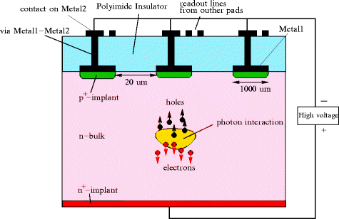
Fig. 11.5
Schematic illustration of silicon as position-sensitive photon detector with sketched device geometry, application of high voltage, and carrier movement for a photon interaction
The detector thickness is modified from the standard particle detectors. A thickness between 0.5 and 1 mm is a good compromise between efficiency, timing resolution, channel count, and limitation of planar detector processing. With attenuation coefficient of μ = 0.2 cm−1 for 511-keV photons, a 1-mm-thick detector stops about 2 % of incoming photons. With standard PET detector elements being nearly 100 % efficient, five or more detector layers must be used to reach the desired 10 % ratio of high-resolution events in the sample.
The detector is reversely biased to voltages exceeding the full depletion voltage, depleting the detector of thermally generated free carriers. An interaction in the detector produces countable pairs of free electrons and holes, the number of which is proportional to the energy deposited by the interacting particle. The generated charge is driven by the electric field to induce signal on electrodes attached to the pads.
The signals collected on the electrodes (105 electrons) are relatively small compared to the signals in the standard PMT-based PET detectors (109 electrons), which makes silicon signals noise prone. This requires dedicated low-noise readout electronics placed very close to the sensors.
11.3.2 The PET Probe Module
The MADEIRA PET probe was constructed of several identical, largely autonomous modules.
The MADEIRA probe module, photographed in Fig. 11.6, is composed of a pair of silicon detectors, each measuring 40 × 26 mm2 and 1 mm thick. Only the top detector is seen in the photograph, the bottom one is exactly behind it, with an approximate spacing of 0.8 mm between the detectors. This spacing is to be small to maximize content of active material in the probe. Each detector is segmented to 1 × 1-mm2 square pads, totalling 1,040 sensitive voxels per sensor, each of 1-mm3 volume and independent from one another.
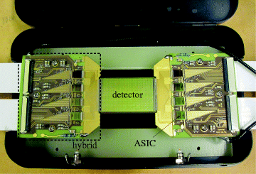
Fig. 11.6
Photograph of a silicon module used as a building block of the silicon PET probe
The detectors are attached to the hybrids, printed circuit boards (PCBs) that provide mechanical support for the detectors and host the first stage of electronic processing. We used VATAGP7, application-specific integrated circuits (ASICs) made by IDEAS [15] for front-end electronics. Each VATAGP7 chip hosts 128 identical parallel processing channels, each channel composed of a low-noise charge-sensitive preamplifier, whose output is split to a pair of electrically separated CR-RC shapers with different shaping times. The fast shaper with a shaping time of 150 ns serves as an input to a leading edge discriminator (one per channel) with a common chip threshold. A fine adjustment of thresholds for each channel is available through onboard digital-to-analog converters (DACs). A logical OR function of all trigger signals from all channels within a chip gives the chip trigger. The slow shaper with a shaping time of 500 ns provides an analog signal corresponding to the number of electron holes collected in this pad or equivalently to the deposited energy. The analog signals are placed in an on-chip shift register. The shift register can be read in a serial mode, when signals collected in all channels on the chip are read sequentially by clocking through the register, or in a sparse readout mode, when only energy of channels that gave a trigger are read from the shift register.
In total, 16 ASICs are required to read the 2,080 pads of both silicon sensors. These are split among four identical PCB boards. A flat cable connector connects the ASICs to the downstream electronics.
11.3.3 The Data Acquisition System
The task of the data acquisition system (DAQ) is to manage the data coming from the probe and interface it to the external ring. On top of that, the DAQ should provide a way to set the operating conditions of the probe. Because of the modular approach, the DAQ should be scalable as well.
For the prototype, a dedicated DAQ system was constructed under a name of MADDAQ [16], depicted in Fig. 11.7. Each MADDAQ board serves one probe module and interfaces directly into a personal computer (PC) via an Ethernet cable. The Ethernet protocol offers an attractive way of multiplying the MADDAQ boards with minimum hardware overhead. Each board is powered with laboratory voltage supplies (+3.3 V and −3.3 V required) and also powers the remote ASICs. The reverse bias voltage of 200 V for the sensors bypasses the MADDAQ and is provided directly to the modules.
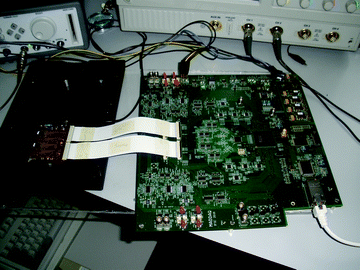
Fig. 11.7
Photograph of a MADDAQ board attached to a test hybrid
The MADDAQ board was built around a field programmable gate array (FPGA) called Spartan-3 from Xilinx [17]. The FPGA and associated circuitry provide the following features:
A trigger logic implementation. The trigger from the external ring and the triggers from the VATAGP7 chips are combined, and coherence is tested, via a standard coincidence time window or through a more complex trigger algorithmRelated posts:

Stay updated, free articles. Join our Telegram channel

Full access? Get Clinical Tree