(3.1)
where A 0 is the initial activity. The isotopes are chosen so that their half-lives reflect the metabolic processes that are being investigated; in any case, half-lives between hours and days at most are suitable. Table 3.1 lists half-lives of radionuclides commonly used in nuclear medicine.
Table 3.1
List of common radionuclides for imaging in nuclear medicine
Nuclide | Mode | Photon energy (keV) | Half-life | Imaging modality |
|---|---|---|---|---|
11C | ß + | 511 | 20.37 min | PET |
13N | 9.97 min | |||
15O | 2.04 min | |||
18F | 109.7 min | |||
82Rb | 76.4 s | |||
67Ga | EC | 93, 185, 300 | 3.26 days | SPECT |
99mTc | IT | 140 | 6.01 h | |
111In | EC | 172, 247 | 2.81 days | |
123I | EC | 159 | 13.2 h | |
125I | EC | 27–30 | 59.4 days | |
201Tl | EC | 68–80 | 3.04 days |
Specific activity. The specific activity is the activity of the sample divided by its mass. For minimum interference, the specific activity injected should be as high as possible. Although specific activity of radionuclides can be very high (≈GBq/pmol), the specific activity of radiopharmaceuticals is much lower due to chemical contamination of sample with nonradioactive isotopes of the radionuclide.
Purity. Purity is the portion of activity sourced by the desired compound. Purity should be high, since the remaining radioactivity will (a) expose patients to redundant radioactive dose and (b) add noise to detection. Notorious example is a well-controlled contamination of 99mTc with its parent 99Mo during extraction from generator.
Chemical properties. The radiopharmaceuticals must mimic all relevant properties of the equivalent pharmaceutical, and elaborate procedures were established to this end. The common methods are a direct replacement, where radioactive isotopes are used in place of their stable counterparts, like 11C for 12C in 11C-choline; creation of analogs, most notably 18F-FDG as a glucose analog; and chelation, e.g., binding of 99mTc in non-active parts of a complex substance.
Production. Radioactive sources are produced in nuclear reactors through chemical purification of fission products or activation and, on a smaller scale, in cyclotrons. For convenience, generators, i.e., long-lived parents of interesting nuclides (99Mo for 99mTc or 82Sr for 82Rb) are shipped from remote nuclear reactors to medical facilities. Conversely, cyclotrons are commonly installed at the facilities themselves to provide on-site access to short-lived PET radionuclides (Table 3.1).
3.3 Detection of Radiation
Detectors for nuclear medicine are optimized for detecting γ radiation in 140–511 keV energy range. In this section we will give an overview of the most common interaction types of photons in this energy range and list sensitive materials used for their detection.
3.3.1 Interactions of Photons with Matter
The passage of photons through matter is marked by discrete, point-like interactions. As a consequence, some photons can pass through obstacles unchanged, and it is only their number that diminishes. For an incident current j 0 of photons on a target of thickness d, the outbound current j will be

where μ is the material specific attenuation coefficient.
(3.2)
Figure 3.1 illustrates the interactions that dominate the specified energy range: the Compton scattering (CS) and the photoelectric effect (PE), each contributing a partial attenuation coefficient to the total attenuation coefficient μ = μ C + μ pe.
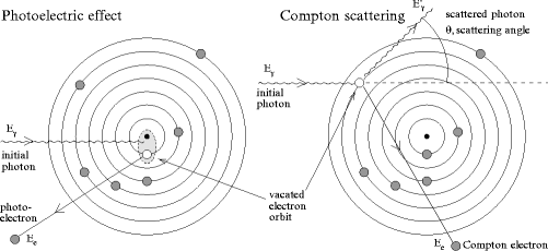
Fig. 3.1
Schematic representation of the most common interactions for photons used in medical imaging: photoelectric effect (left) and Compton scattering (right)
In the photoelectric effect, the photons are completely absorbed in the electric field of the target nucleus (see Fig. 3.1, left). The energy of the photon is transferred to an electron from the atomic shell of the target atom. The emitted electron is referred to as the photoelectron, and its kinetic energy is equal to the energy of the incident photon minus its binding energy. Since the nucleus is involved in the interaction, probability for PE is higher for electrons in strongly bound shells close to the nucleus. When the energy of the incoming photons exceeds the binding energy of those shells, a sharp rise in the partial attenuation coefficient μ pe can be observed in Fig. 3.2. The most energetic of those edges corresponds to the K-shell transitions, where electrons from the innermost shells (1 s) of the target atoms are excited. Above the K threshold, the attenuation coefficient scales as
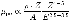
with ρ, A, and Z being the density, mass, and atomic numbers of the target material and E the energy of the incoming photon. The exponents for Z and E vary within the energy range of photons used in imaging. Note the strong Z dependence and the sharp drop with increasing energy of the photons.
(3.3)
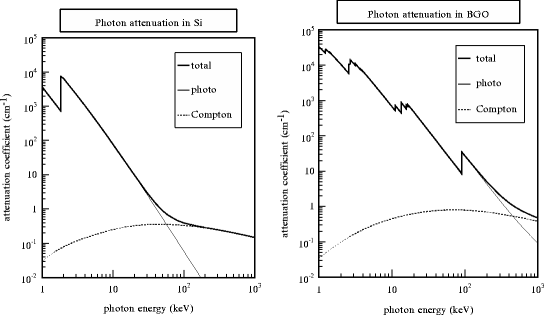
Fig. 3.2
Attenuation coefficient for photons in Si (left) and BGO (right). Note the logarithmic scales
The Compton scattering is an elastic scattering of a photon with an electron in the atomic shell. The energy transfer between the particles is sufficient to excite the electron, called a Compton electron, from the atom. Since other particles, including the nucleus, can be considered as spectators only, a relation between the scattering angle θ of the photon and the transferred energy E e can be derived:
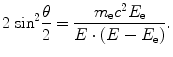
(3.4)
The quantum effects do not extend to the scattering angle, which is a continuous variable. As a consequence, the spectrum of the emitted electrons is a continuum with a sharp drop, the Compton edge, corresponding to the maximum energy transfer at backscattering. The partial attenuation coefficient μ C is proportional to

and has, conversely to μ pe, a weak relationship to Z and little variation with energy over the given range.
(3.5)
Figure 3.2 illustrates both partial and total attenuation coefficients in two materials, one with a low Z (Si, left) and one with a high Z (BGO, right), which span the range of sensors and materials used in nuclear medicine detection. The strong PE energy dependence breaks the photon interactions to two regions. By labeling E q as the energy where μ C(E q) = μ pe(E q), the photons with energy below E q will be predominantly photoelectrically absorbed, while above E q, they will undergo CS, with a narrow region where both processes are equally probable. Below E q, because of the Z dependence of μ pe, there will be huge difference in attenuation coefficient in different media: at 30 keV for Si with μ = 3 cm−1 and BGO with μ = 170 cm−1 the difference is almost two orders of magnitude. Above E q, μ predominantly scales with ρ, since Z/A ≈ 1/2 for most materials, resulting in variation confined to less than one order of magnitude.
3.3.2 Sensitive Materials: Scintillators
Scintillators are materials that convert ionization to visual light [2]. For detection of gamma radiation, the signal is produced in two stages—the incident photon undergoes one of the interactions mentioned above to create an electron with substantial kinetic energy, be it Compton- or photoelectron, and then the electron’s energy is converted to countable photons of visual light. Table 3.2 lists some properties of common scintillators used in nuclear medicine. The most commonly used scintillator material is NaI, being relatively inexpensive and malleable. For PET, detection efficiency is crucial, and devices are based on BGO (chemically Bi4Ge3O12) or L(Y)SO. The name L(Y)SO describes two distinct crystals—proprietary LSO (Lu2SiO5), and an open source LYSO, which is a 10 % admixture of YSO (Y2SiO5). Both have nearly identical properties and will be treated as a single substance throughout the text.
Material | Yield (ph/keV) | 140 keV | 511 keV | Decay time (ns) | ||
|---|---|---|---|---|---|---|
d 1/2 (mm) | CS/PE | d 1/2 (mm) | CS/PE | |||
NaI | 38 | 2.83 | 0.18 | 21.46 | 4.6 | 230 |
BGO | 8 | 0.59 | 0.06 | 7.65 | 1.3 | 300 |
L(Y)SO | 32 | 0.75 | 0.09 | 8.55 | 1.9 | 40 |
CsI | 52 | 1.92 | 0.15 | 16.93 | 3.5 | 1,000 |
BaF2 | 10 | 2.01 | 0.18 | 15.84 | 4.1 | 0.6/620 |
LaBr3 | 63 | 2.61 | 0.26 | 16.11 | 6.3 | 16 |
The important parameters of scintillators are (see Table 3.2):
Photon yield. Number of visual photons created per keV kinetic energy of the electron. Higher numbers indicate larger signals enabling better energy and timing resolution. Note advantage of recent engineered materials like L(Y)SO or LaBr3 over BGO.
Detection efficiency. The efficiency of a material can be expressed through the half-value thickness (d 1/2 = ln(2)/μ), which is the thickness of material required to detect half of the incoming photon flux. It should be considered that only photons interacting through PE will contribute to the image (Sect. 3.4.3); therefore, it is desirable that the relative Compton scattering probability is small compared to photoelectric effect. Table 3.2 states d 1/2 and the ratio (CS/PE) for two most common photon energies, 140 keV of 99mTc and 511 keV of annihilation photons. To maximize efficiency, materials composed of high Z elements (83Bi, 71Lu and 53I) are used, which benefit from the strong Z 4–5 dependence of μ pe. Since μ is proportional to ρ, the materials are also relatively dense, from 3.67 g/cm3 of NaI to 7.3 g/cm3 for L(Y)SO. At the low end of the energy spectra, almost all materials have sufficiently low values of d 1/2 and (CS/PE), so that the other properties become crucial for material selection. At the high end, the efficiency becomes crucial; however, the reign of BGO has been overthrown by the superior light yield and lightningly fast decay time of L(Y)SO.
Decay time. Average duration of light emission after the interaction. A short decay time implies large prompt signals and improves timing resolution. Note the excellent values for L(Y)SO and LaBr3.
Hardly any material is perfect, and the final choice is governed by the requirements of each specific application.
3.3.3 Light Detectors
Scintillators require extremely sensitive photodetectors able to detect single photons. The most common devices are photomultiplier tubes (PMTs), composed of a photocathode and a series of multiplication dynodes (8–12 stages are common). On the photocathode, the visual photons are converted (back) to photoelectrons with the quantum efficiency (QE) measuring the conversion rate of photons to photoelectrons emitted towards the first dynode. For standard PMTs, QE ranges between 1 and 3 photoelectrons for ten initial photons depending on the photocathode composition. Subsequent dynodes multiply the signal to about 106 times the original photoelectron count. Since the electron multiplication is done in vacuum, the PMTs are in general bulky and fragile and very sensitive to all external influences, even the one of the terrestrial magnetic fields.
Silicon-based light detectors were introduced to imaging in nuclear medicine to circumvent some of those difficulties. Figure 3.3 illustrates the principle of operation. The device is a reversely operated diode with graded dopant concentration (n+pπp+). The uneven doping concentration is reflected in the nonhomogeneous electric field, which is strong in the multiplication region and moderate in the active region. Light enters through the bottom entrance window and produces charge carriers in the active region of the device. A moderate field splits the carriers; the electrons are steered towards the high field region and multiplied. Since charge is multiplied within the crystal, no evacuated container is needed and ordinary magnetic fields will not break the multiplication chain. The same charge containment argument makes QE of silicon-based devices larger than the one of PMTs with a common value of 4 or more carrier pairs per 10 visual photons.
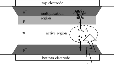
Fig. 3.3
Schematic representation of APD operation
Based on the multiplication factor, two types of devices are constructed:
In avalanche photodiodes or APDs [5], the multiplication factors are between 100 and 1,000, preserving the proportionality of the collected electron current to the incoming light flux. This multiplication factor is at least an order of magnitude smaller than in PMTs, which is normally not a problem, but its strong dependence on temperature, applied voltage, and device nonuniformity is. The timing resolution depends on the multiplication and is also slightly worse than in PMTs.
The silicon photomultipliers or SiPMs [6] operate in Geiger mode, each photon interaction generating a complete device discharge. To keep proportionality, the device is split into tiny cells, squares with sides between 25 and 100 μm. The proportionality is broken when multiple photons interact in a single cell and get counted as a single photon. The dynamic range is limited by the number of cells per device; however, the saturation effects are tolerable, since the devices are generally small (1–10 mm2) to limit their capacitance and to allow decent timing, and are finely segmented to as much as few thousands of cells per device. Present devices are extremely sensitive to changes in operating conditions, most notable the applied reverse voltage and ambient temperature. Furthermore, the small cell size implies complex readout and electronics.
3.3.4 Sensitive Materials: Solid-State Detectors
Solid-state detectors are modified semiconductor devices. Most sensors are reversely operated diodes, segmented to the desired resolution. The reverse bias depletes the sensor of thermally generated carriers. As a photon strikes the detector and creates a Compton or a photoelectron, the energy of the emitted electron is converted into a countable number of electron–hole pairs. The electron–hole pairs are split in the applied reverse bias and collected to respective electrodes.
In general, the number of created pairs in semiconductors, given in Table 3.3, supersedes the yield of scintillators (Table 3.2), giving excellent energy resolution. The diodes can be made to almost arbitrarily small sizes, and resolutions down to 1 μm were measured [7]. The solid-state detectors are currently found in applications where energy or spatial resolutions are crucial (e.g., small animal imaging, Compton camera, high precision scanners [8,9]). The relatively long charge collection times and available manufacturing algorithms favor thinner sensors. To match scintillator efficiencies, multiple layers of segmented sensors have to be used, increasing channel count and device complexities.
Table 3.3


Properties of semiconductors being introduced in nuclear medicine: material, yield given as number of carriers per keV energy loss of the initial electrons, half-value length d 1/2 and ratio of probabilities CS/PE for Compton scattering versus photoelectric effect, both at 140 and 511 keV photon energy and approximate collection times (they depend on operating conditions and material thickness)
Related posts:

Stay updated, free articles. Join our Telegram channel
Full access? Get Clinical Tree