Chapter 15 Semiconductor materials
Chapter contents
15.1 Aim
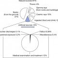
This chapter introduces the reader to semiconductors and semiconducting devices that are important to radiography. This is a very large field, and the chapter concentrates on the barrier layer rectifier, which has made a major impact on radiographic science. After an overview of the development and manufacture of integrated circuits. the chapter concludes with an overview of the used of semiconductor devices in radiography.
15.2 Introduction
Other, simpler, solid-state devices are widely used in X-ray circuitry and are suitable for inclusion in this chapter after a general description of the properties of semiconductor materials.
15.3 Intrinsic semiconductors
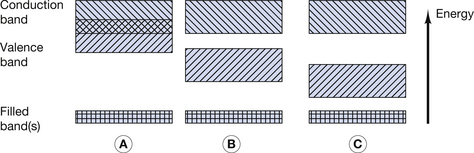
An intrinsic semiconductor is a chemically pure semiconductor, which is also assumed to have perfect regularity of atoms within its crystalline structure or lattice. The concept of semiconducting materials was briefly introduced in Section 7.3.2 where the properties of conductors, insulators and semiconductors were compared in terms of the energy band model for the orbiting electrons. This was illustrated in Figure 7.2 and this diagram is reproduced here as Figure 15.1 (below). As shown in Figure 15.1B, one of the characteristics of semiconductors is that there is a small energy gap (up to a few eV) between the top of the valence band and the bottom of the conduction band. At very low temperatures, all the outer electrons have energies near the bottom of the valence band, and no electrons are able to take part in electrical conduction, as there are no free electrons in the conduction band. As mentioned in Chapter 7, increasing the temperature of a semiconductor increases its conductivity. At normal room temperatures, many electrons are able to gain sufficient energy (because of the increased kinetic energy of the atoms) to jump up to the conduction band and so take part in electrical conduction.
15.3.1 Positive holes
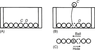
1. Electrons are being excited into the conduction band creating holes in the valence band.
2. There is movement of electrons in the conduction band and holes in the valence band.
3. There is a recombination of electrons in the conduction band with holes in the valence band.
15.3.2 Silicon
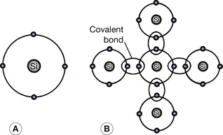
Silicon is currently the most widely used general semiconductor material. It has an atomic number of 14 and has 14 protons in its nucleus and 14 electrons orbiting that nucleus (see Ch. 18). This means that the two inner shells (K– and L-shells) are completely full and contain two and eight electrons respectively. The next shell out from the nucleus is the M-shell and this exhibits a stable configuration when it contains either eight or 18 electrons (see Ch. 18). In this case, it contains four electrons and so may be regarded as an incomplete shell in the solitary silicon atom. However, in the silicon crystal there is a regular arrangement of atoms in which each silicon atom shares its outer electrons with four neighboring atoms so that each atom appears to have eight electrons in its M-shell and thus stability (see Fig. 15.2). Such electron bonds are known as covalent bonds and the electrons are termed valence electrons and inhabit the valence energy band of the atom. The covalent bonds give the crystal its regularity by inhibiting the movement of any particular atom. At room temperature, these bonds are being continuously broken and reformed as some of the valence electrons are gaining sufficient energy to reach the conduction band (bond broken) and electrons from the conduction band fall back into the valence band (bond reformed). The eight-electron configuration of the M-shell behaves like a full shell and so the valence band is effectively full until an electron moves up to the conduction band. As previously explained, when this happens, electron flow in the conduction band and positive-hole flow in the valence band are both possible.
15.4 Extrinsic semiconductors
15.4.1 N-type semiconductors
As we have seen, single atoms of intrinsic semiconductors have four valence electrons. To produce an N-type extrinsic semiconductor, a pentavalent impurity (one with five valence electrons) is used as the doping material. Arsenic, antimony and phosphorus are examples of pentavalent elements that are suitable. Figure 15.3 (See page 96) illustrates the effect of introducing an atom of phosphorus into the crystalline structure of silicon. Four of the valence electrons in the phosphorus form covalent bonds and the fifth electron is unbonded. This electron has an energy level which is just below the bottom of the conduction band (see Fig. 15.3B). At normal room temperatures, it is therefore virtually a free electron since it is easily lifted into the conduction band and can take part in electrical conduction if a potential difference is applied across the crystal.
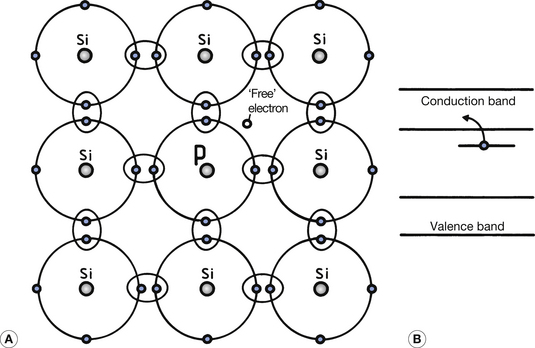
Since such pentavalent atoms provide a ‘spare’ electron, they are known as donor impurities. It must be remembered that some electrons from the valence band will also be able to jump into the conduction band due to the normal vibrational energy within the atom at room temperature (this is similar to the intrinsic semiconductor; see Sect. 15.3). Positive holes will also be produced in the valence band and add to the conductivity. At normal room temperatures, this effect is much less than the effect produced by the donor atoms. In the case of an N-type semiconductor, the majority carriers are the electrons in the conduction band and the minority carriers are the holes in the valence band.