TFT Flat-Panel Array Image Acquisition
Objectives
On completion of this chapter, you should be able to:
• Define a thin-film transistor (TFT) flat-panel digital image detector.
• Describe the construction of direct and indirect TFT flat-panel detector systems.
• Differentiate between direct and indirect image capture.
• Describe a gadolinium oxysulphide (Gd2O2S) detector.
• Describe a thallium doped cesium iodide (CsI[TI]) detector.
• Relate the design of a TFT flat-panel detector to its performance measurements.
• Describe the cause of image lag and the process of correcting.
Key Terms
Active-matrix flat-panel imagers (AMFPI)
Direct conversion
Field effect transistor (FET)
Flat-panel detector
Gadolinium oxysulphide (Gd2O2S)
Gain calibration
Hydrogenated amorphous silicon (a-Si:H)
Image artifacts
Image lag
Indirect conversion
Offset correction
Photoconductors
Sensing component
Switching component
Thallium doped cesium iodide (CsI[TI])
Thin-film transistor (TFT)
The first thin-film transistor (TFT) flat-panel amorphous silicon and amorphous selenium detectors were introduced in 1995. These were the first devices to move beyond the cassette into detectors that would reside in the table and wall stand. Today these detectors are no longer permanent fixtures in these two pieces of equipment but can be used portably as a wireless device. With flat-panel detectors, the materials used for detecting the x-ray signal and the sensors for recognizing that signal are permanently enclosed inside a rigid protective housing. This chapter will explore these devices and differentiate between the two major types of x-ray signal conversion: indirect and direct.
Active-Matrix Flat-Panel Imagers
Active-matrix flat-panel imagers (AMFPI) consist of a flat-panel array with an x-ray absorption material. The two main types of x-ray absorption materials currently being used are photoconductors and scintillators. Photoconductors are materials that absorb x-rays, resulting in an electrical charge. Scintillators are phosphors that produce light when absorbing x-rays. An AMFPI detector measures the response of these materials to x-ray absorption and is a large area two-dimensional (2-D) array of pixels fastened to a thin glass backing, or substrate. The absorption material is attached to the surface of this array either electrically, as in the case of the photoconductor, or physically, as in the case of the phosphor material. The 2-D array functions as a very efficient device that measures x-ray absorption rather than counting or measuring the actual x-rays. The choice of x-ray absorption material determines whether the detector is direct conversion or indirect conversion.
Direct Conversion
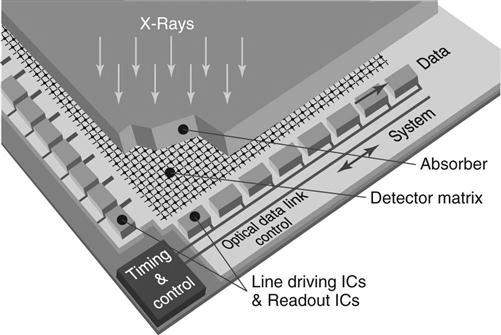
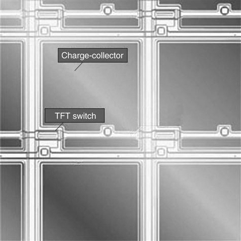
In direct conversion, x-ray photons are absorbed by the coating material and immediately converted into an electrical signal. The flat-panel detector has a radiation-conversion material or photoconductor, typically made of amorphous selenium (a-Se) that is about 500 µm thick for radiography and 200 to 250 µm thick for mammography. This material absorbs x-rays and converts them to electrons, which are stored in the TFT detectors (Figure 5-1). The TFT is a photosensitive array made up of small (about 100 to 200 µm) pixels, also called a detector element (del) in these TFT arrays. Each pixel contains a photodiode that absorbs the electrons and generates electrical charges. A field effect transistor (FET) or silicon TFT isolates each pixel element and reacts like a switch to send the electrical charges to the image processor (Figure 5-2). More than 1 million pixels can be read and converted to a composite digital image in less than 1 second. A line of TFT switches, each associated with a storage capacitor, allows the electrical charge information to discharge when the switches are closed. The information is discharged onto the data columns and read out with dedicated electronics. Specialized silicon integrated circuits are connected along the edges of the detector matrix. On one side, integrated circuits control the line scanning sequence, and on the other side, low-noise, high-sensitivity amplifiers perform the readout, amplification, and analog-to-digital conversion. High-speed digital electronics are then used to achieve fast image acquisition and processing.
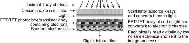
Indirect Conversion
Indirect-conversion detectors are similar to direct detectors in that they use TFT technology. Unlike direct conversion, indirect conversion is a two-step process: x-ray photons are converted to light, and then the light photons are converted to an electrical signal. A phosphor such as gadolinium oxysulphide (Gd2O2S), or thallium doped cesium iodide (CsI[TI]) rapidly absorbs x-rays and produces light. The phosphor layer is known as the scintillation layer. The scintillation layer can be either structured or unstructured. Unstructured layers produce more scattered light than structured layers, thereby decreasing the efficiency of the detector. The light is then converted into an electric charge by a photodetector such as a hydrogenated amorphous silicon (a-Si:H) photodiode array. The two-step process occurs as follows:
Step 2: A photosensitive array, made up of small (about 100 to 200 µm) pixels, converts the light into electrical charges. Each pixel contains a photodiode that absorbs the light from the scintillator and generates electrical charges. A FET or silicon TFT isolates each pixel element and reacts like a switch to send the electrical charges to the image processor. As with direct conversion, more than 1 million pixels can be read and converted to a composite digital image in less than 1 second (Figure 5-3).