CCD/CMOS Image Capture
Objectives
On completion of this chapter, you should be able to:
• Describe the components of a charge-coupled device (CCD).
• Explain the function of a CCD.
• Define complementary metal oxide semiconductor (CMOS).
• Describe the basic construction and function of a CMOS.
Key Terms
Amplification noise
Analog-to-digital converter (ADC)
Blooming
Bucket brigade scheme
Charge-coupled devices (CCDs)
Complementary metal oxide semiconductor (CMOS)
Dark current noise
Detector element (del)
Dopants
Fiber optics
Gadolinium sulfur dioxide scintillator
Lenses
N-type transistors
Polysilicon layer
P-type transistors
Quantum efficiency
Semiconductor
Silicon dioxide layer
Silicon substrate
Spectrum sensitivity
Statistical noise
Charge-Coupled Devices (CCDs)
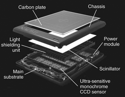
The oldest indirect-conversion digital radiography systems used charge-coupled devices (CCDs) to acquire the digital image. These devices are still being used in a variety of image capture applications. In a CCD system, x-ray photons interact with a scintillation material and the signal is transmitted by lenses or fiber optics to the CCD. During the transmission process, the lenses reduce the size of the projected visible light image and transfer the image to one or more small capacitors that convert the light into an electrical charge. This charge is stored in a sequential pattern and released line by line and sent to an analog-to-digital converter (ADC) (Figure 6-1).
Structure and Function
A photosensitive receptor and electronics embedded into a substrate material in a silicon chip make up a CCD. Incident light from a scintillator strikes the detector and electron/hole pairs are produced in the silicon. The number of electron/hole pairs is related to the amount of light that is absorbed. The electrons are held by electrostatic forces in the array until the charge is read out to form the image. The chip is made up of a polysilicon layer, a silicon dioxide layer, and a silicon substrate (Figure 6-2). The polysilicon layer is coated with a photosensitive material and contains the electronic gates. The silicon dioxide layer is an insulator and the silicon substrate contains the charge storage area.
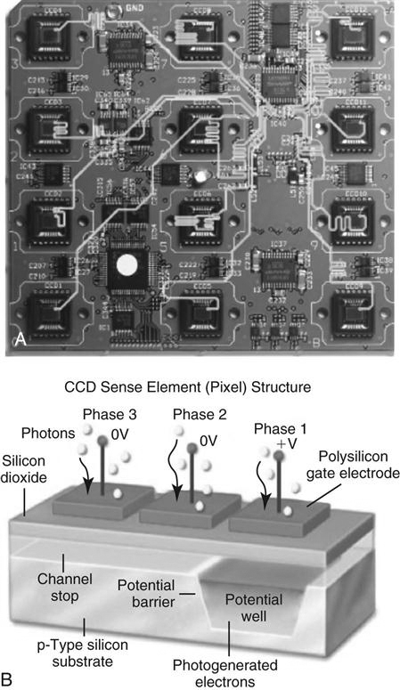
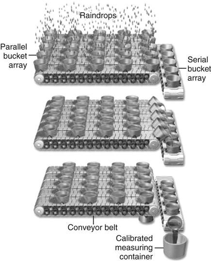
Each pixel or detector element (del) contains three electrodes that hold the electrons in a electrical potential well. The dels are formed by voltage gates that, at readout, are opened and closed like gates to allow the flow of electrons. To collect the charge on the silicon chips, the voltage sign is changed on the electrodes within each del, moving the electrons by rows down the columns until the readout row is reached. This process is commonly known as the “bucket brigade scheme” (Figure 6-3). Once the readout row is reached, the data are sent sequentially to the sense amplifier and are then digitized. The readout process requires that the movement of the electrons is timed, and multiple voltage changes occur; however, the process is very quick. There can be issues with overfill in the dels, which causes excess electrons to spill out of the del into an adjacent del. This is handled by building overflow drains into the array to reduce or prevent this “blooming” effect.
Image-Related Characteristics
Because of the high cost of a CCD chip, it is not practical to manufacture CCD chips any larger than 5 cm × 5 cm. Most chips range from 2 to 4 cm. The image has to be matched to the size of the CCD, which implies that the image must be reduced in size. To do this, CCD technology uses lenses or fiber optics so that the image matches the receptor size. Reducing the image size involves several factors that contribute to the quality of the image and each must be considered. These factors include the scintillator, light collection components, and noise.
The Scintillator.
The type of scintillator and the way it is constructed will determine how much of the incident x-ray photons are absorbed, how much light is produced, and the wavelength or color of the light. Remember from Chapter 5
Stay updated, free articles. Join our Telegram channel

Full access? Get Clinical Tree


