(1)
Cleveland Clinic, Emeritus Staff, Cleveland, OH, USA
Keywords
DetectorsBlock detectorsPETPET/CTPET/MRAnimal scannerBackground
The detection and measurement of radiation is based on the interaction of radiations with matter discussed in Chap. 1. In gases, ionizing radiations, particulate or electromagnetic, interact with gas molecules to produce positive and negative ions, which are then collected as current or count by the application of a voltage. The amount of ionization is proportional to the amount of energy deposited by the radiation. At low voltages, the ionization is measured as current that is proportional to the amount of radiation. Dose calibrators, pocket dosimeters, and ionization chambers operate on this principle at low voltages (∼150 V). At high voltages (∼900 V), ions are multiplied in an avalanche of interactions producing a pulse that is independent of the energy and type of radiation. Each event of interaction is detected as a count, and this principle is applied in Geiger–Müller (GM) counters, which are used as radiation survey meters.
Liquid scintillation detectors operate on the principle of interaction of radiations with a special type of scintillating liquid that emits light upon interaction with radiation. The light is then processed in the same manner as in the case of a solid detector, as discussed below.
Both gas and liquid scintillation detectors have low detection efficiency and, therefore, are not used in PET technology. Interaction of radiations with solid scintillation detectors is the basis of radiation detection in PET technology. These solid detectors have the unique property of emitting scintillation or flashes of light after absorbing γ– or X-ray radiations. The light photons are converted to an electrical pulse or signal by a photomultiplier (PM) tube. The pulse is further amplified by a linear amplifier, sorted by a pulse height analyzer (PHA), and then registered as a count. Different types of radiations are detected by different types of detectors. For example, γ-rays or X-rays are detected by sodium iodide crystal containing a trace amount of thallium, NaI(Tl), whereas organic scintillation detectors such as anthracene and plastic fluor are used for β − particle detection. PET is based on the detection of two 511-keV photons in coincidence at 180°. These photons are produced by the annihilation process in which a positron emitted by a positron-emitting radionuclide combines with an electron in the medium and is annihilated. Solid scintillation detectors of different materials have been investigated to detect 511-keV photons. Semiconductor detectors are different kind of solid detectors, which produce electron-hole pairs upon interation with radiations, followed by application of a voltage to produce current. The following is a brief description of the properties and uses of solid detectors in PET imaging.
Solid Scintillation Detectors
Although many scintillation detectors have been investigated, only a few have been widely used in PET technology. The characteristics of different detectors that have application in PET technology are listed in Table 2.1. Note that photon yield from pure detectors is normally poor and so most of them are fabricated with trace amount of a doping element to improve the photon yield. Sodium iodide is doped with a trace amount of thallium (Tl), whereas most others are doped with cerium (Ce). There are several methods of fabrication, but the basic principle is as follows: the detector material and the doping agent in oxide form are mixed in appropriate ratio (e.g., lutetium oxide and cerium oxide) and melted in an iridium crucible, which is heated by a water-cooled induction coil. Crystal growth is initiated on seed crystals which are then pulled out at a controlled rate to form the crystals of desired size.
Table 2.1
Properties of different solid scintillation detectors
Detectors | Effective atomic no (Z) | Density (g/cm3) | Scintillation decay time (ns) | Photon yield (per keV) | Linear attenuation coefficient (cm−1) of 511 keV | Energy resolution (% at 511 keV) |
|---|---|---|---|---|---|---|
NaI(Tl) | 51 | 3.67 | 250 | 38 | 0.34a | 7.8 |
BGO | 74 | 7.13 | 300 | 6 | 0.96 | 20 |
BaF2 | 54 | 4.89 | 0.6 | 2 | 0.44 | 11.4 |
GSO | 59 | 6.71 | 50 | 10 | 0.67 | 9.5 |
Anthracene | – | – | 26 | 30 | – | – |
LSO | 66 | 7.40 | 40 | 29 | 0.87 | 10.1 |
YSO | 34 | 4.53 | 70 | 46 | 0.39 | 12.5 |
CsI(Tl)b | 54 | 4.51 | 1000 | 52 | 0.483 | 4.53 |
LYSO | 65 | 7.2 | 50 | 25 | 0.87 | 20 |
YAP | 39 | 5.4 | 27 | 18 | 0.46c | 2.5 |
LaBr3 | 47 | 5.3 | 25 | 61 | 0.47 | 5.3 |
The choice of a detector is based on several characteristics, namely:
1.
Stopping power of the detector for 511-keV photons
2.
Scintillation decay time
3.
Light output per keV of photon energy
4.
Energy resolution of the detector
The stopping power of the detector determines the mean distance the photon travels until complete deposition of its energy and depends on the density and effective atomic number (Z eff) of the detector material. The scintillation decay time arises when a γ-ray interacts with an atom of the detector material, and the atom is excited to a higher energy level, which later decays to the ground state, emitting visible light. Two to sixty light photons are produced per keV of incident energy depending on the type of detector material (Table 2.1). The time of decay is called the scintillation decay time given in nanoseconds (ns) and varies with the material of the detector. The shorter the decay time, the higher the efficiency of the detector at high count rates. A high-light-output detector produces a well-defined pulse resulting in better energy resolution. The intrinsic energy resolution is affected by inhomogeneity in the crystal structure of the detector and random variations in the production of light in it. The energy resolutions at 511 keV in different detectors vary from 2.5 to 20% (Table 2.1), using routine integration time for pulse formation, which runs around a few microseconds. However, in PET imaging, the integration time is a few hundred nanoseconds in order to exclude random coincidences, and the number of photoelectrons collected for a pulse is small, thus degrading the energy resolution. Consequently, the detectors in PET scanners have relatively poorer energy resolution (∼12%) (See later in Table 2.2).
Table 2.2
Features of different PET scanners
Manufacturers→a | Philipsb | Siemensc | GE Healthcarec | |||
|---|---|---|---|---|---|---|
GEMINI TF Big Bore | GEMINI TF 64 (PET/CT) | Biograph mCT | Biograph TruePoint | Discovery VCT | Discovery PET/CT 600 | |
Models→ | ||||||
Features↓ | ||||||
Number of detectors | 28 pixelar modules | 28 pixelar modules | 192 | 192 | 24 rings | 24 rings |
Number of crystals | 28,336 | 28,336 | 24,336 | 24,336 | 13,440 | 12,288 |
32,448 (TrueV) | ||||||
32,448 (TrueV) | ||||||
Detector material | LYSO | LYSO | LSO | LSO | BGO | BGO |
Ring diameter (cm) | 90 | 90 | 84.2 | 83 | 88.6 | 81 |
Patient scan range (cm) | 190 | 190 | 190 | 190 | 160 | 170 |
Crystal size (mm) | 4 × 4 × 22 | 4 × 4 × 22 | 4 × 4 × 20 | 4 × 4 × 20 | 4.7 × 6.3 × 30 | 4.7 × 6.3 × 30 |
Number of PMTs | 420 | 420 | 4/block | 4/block | 280 | 256 |
Energy resolution (%) | 12% | 11.7% | 12% | 12% | – | – |
Coincidence window (ns) | 5 | 3.8 | 4.1 | 4.5 | 10 | 10 |
Axial FOV (cm) | 18 | 18 | 16.2/21.6 | 16.2/21.6 | 15.7 | 15.7 |
Acquisition mode | 3D, 4D, TOF | 3D, 4D, TOF | 3D | 3D | D, 3D, 4D | 3D, 4D |
The detection efficiency of a detector is another important property in PET technology. Since it is desirable to have shorter scan times and low tracer activity for administration, the detector must detect as many of the emitted photons as possible. The 511-keV photons interact with detector material by either photoelectric absorption or Compton scattering, as discussed in Chap. 1. Thus, the photons are attenuated (absorbed and scattered) by these two processes in the detector, and the fraction of incident γ-rays that are attenuated is determined by the linear attenuation coefficient (μ) given in Chap. 1 and gives the detection efficiency. At 511 keV, μ = 0.92 cm−1 for bismuth germanate (BGO), 0.87 cm−1 for lutetium oxyorthosilicate (LSO), and 0.34 cm−1 for NaI(Tl) (Melcher 2000). Consequently, to have similar detection efficiency, NaI(Tl) detectors must be more than twice as thick as BGO and LSO detectors.
Sodium iodide: For γ-ray detection, NaI(Tl) detectors are most commonly used, as they provide good light output (30–40 light photons per keV of γ-ray energy) and energy resolution. They are most widely used in most gamma cameras for planar or single-photon emission computed tomography (SPECT) imaging in nuclear medicine. The NaI(Tl) crystal is hygroscopic and, therefore, hermetically sealed with aluminum foil. It is fragile and needs careful handling. Its major drawback is its poor stopping power, i.e., low density and low linear attenuation coefficient for 511 keV. For this reason, though used in earlier PET scanners, it has not received much appreciation for application in PET technology.
Bismuth germanate: BGO detectors are preferred in some PET cameras because of its highest stopping power (highest density and linear attenuation coefficient). However, it suffers from its longer scintillation decay time (~300 ns) and poor light output. The longer decay time increases the dead time of the detector and limits the count rate that can be detected by the system. The low light output results in poor energy resolution, which is proportional to the square root of the number of scintillation photons and is typically 20% for 511-keV photons. Note that BGO does not contain any doping material.
Lutetium oxyorthosilicate: The three characteristics of cerium-doped LSO, namely, high light output, high stopping power (high-density and large linear attenuation coefficient), and short scintillation decay time (40 ns), have made it a better detector for PET systems. However, owing to its intrinsic property, its energy resolution is poor despite its high light output. A disadvantage of this detector is that it contains a naturally occurring radioisotope of its own, 176Lu, with an abundance of 2.6% and a half-life of 3.8 × 10⁸ years. This radionuclide decays by emission of β −rays and X-rays of 88–400 keV. However, the activity level is too little to be concerned about radiation exposure from 176Lu, and it does not pose any problem in PET imaging because its photon energy is lower than 511 keV.
Gadolinium oxyorthosilicate: The overall characteristics of cerium-doped gadolinium oxyorthosilicate (GSO) detectors are quite good for application in PET technology. Even though it has lower light output and stopping power than the LSO detector, its better energy resolution has prompted some commercial manufacturers to use this detector in PET technology. Fabrication of GSO detectors requires great care, because the crystals are fragile. GSO detectors collect data faster than other materials and hence are often called “fast crystal.” These detectors can be cut into smaller crystals resulting in improved spatial resolution of the system.
Barium fluoride: Like BGO, BaF2 too does not contain any doping material. It has the shortest decay time of 0.6 ns and is excellent for time-of-flight scanners. In the past its use was limited due to lack of fast computers. With the introduction of fast electronics and computers, they have been used by some investigators for a limited number of clinical studies.
Lutetium yttrium oxyorthosilicate: A somewhat new detector, yttrium-activated lutetium oxyorthosilicate (LYSO), has the physical properties similar to LSO and has been used in PET scanners by a commercial vendor. Its energy resolution is better than LSO’s.
Yttrium oxyorthosilicate: Cerium-doped yttrium oxyorthosilicate (YSO) is a new type of detector, but no commercial manufacturer has yet used it in PET technology.
Lanthanum bromide: Lanthanum bromide (Ce) crystals have high density and hence high stopping power to provide high photon yield upon photon interaction. Also its scintillation decay time is reasonably short (25 ns) to give better energy resolution. All these characteristics make it a potentially good detector for PET scanners. However, there are challenges to its commercial use in PET technology, because it is quite fragile and so difficult to produce large crystals. Furthermore, it is hygroscopic and needs to be hermetically sealed.
Phoswich: For the purpose of increasing spatial resolution in tomographic imaging, two scintillation detectors of different decay times are optically coupled in layers to form a single dual-layered detector, which is connected to a common PM tube (Fig. 2.1). GSO and BGO detectors and NaI(Tl) and LSO detectors have been coupled in this manner for high-resolution scanners. The location of photon interaction is determined from the difference in decay of the pulses from the two detectors, which eliminates the uncertainty in the depth of interaction of the photon thus improving the spatial resolution in images. These detectors can be used in both SPECT and PET scanning by switching between the two detectors.
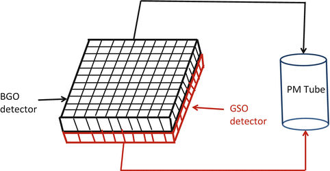
Fig. 2.1
Schematic illustration of phoswich, which is made of two layers of detectors (e.g., BGO and GSO) with different properties
Semiconductor Detectors
Pure silicon and germanium are semiconductor elements that have been used for photon detection. When a γ-ray strikes these elements, an electron is ejected from the atomic orbital and a positively charged hole is created. If a voltage is applied between two electrodes placed in the material, the electron–hole pair will move to the respective electrodes producing a current.
The conductivity of pure metals is poor and adding some impurities or dopants (which are typically elements of low atomic number) to them greatly increases the number of electron–hole pairs in the semiconductor material whereby conductivity is enhanced. When dopants such as boron are added to silicon, doped silicon contains mostly free holes and is called “p-type” semiconductor. Similarly, “n-type” semiconductor possessing more free electrons is obtained by adding dopant like phosphorus to silicon. When these two types of semiconductors are joined together, a unique semiconductor called the PN diode is formed. Since holes and electrons move freely, those at the junction neutralize their charges creating what is called the depletion zone and further free flow of electrons and positive holes across the depletion zone is restricted. When an external voltage is applied connecting the positive polarity to the p-type side and the negative polarity to the n-type side, electron–hole pairs are created and current flows freely and the voltage is called forward bias. When the polarity is reversed, electron–hole pairs are drawn away from the depletion zone and no current flows rendering it a sort of resistor. The voltage is called the reverse voltage.
When radiations of sufficient energy strike the PN diode, they create electron–hole pairs in depletion zone. If a voltage of sufficient energy is applied, holes and electrons move to the respective electrodes creating a current that is proportional to the radiation energy deposited in the detector. PN diodes can serve as photodetectors and research is continuing to employ them in preclinical PET imaging, which hopefully will find use in routine clinical studies.
A variation of PN diode is a PIN diode in which a layer of intrinsic material without any dopant is placed at the p–n junction between the two semiconductors (Fig. 2.2). This increases the depletion region and if a forward bias voltage is applied to the diode, the electron–hole pairs enter the depletion region (including the intrinsic region) and as the two carrier types meet, current starts to flow. Because of the increase in the depletion region with the addition of intrinsic material and concomitant increase in volume in which light conversion occurs, the performance of the PIN diode in photon detection is much improved.
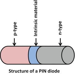
Fig. 2.2
Illustration of the structure of a PIN diode
Because semiconductors are low Z material, their stopping power is low. Also, unlike other scintillation detectors, there is no PM tube multiplication (see later) as there is no light photon produced in the semiconductor material, so the signal (gain of 1) is significantly weaker than the PM tube signal (gain of 106–107). If, however, a reverse bias voltage of sufficient magnitude (200–2000 V) is applied, then the free electron accelerates in the material and can knock out an electron from an atomic orbital creating a second electron–hole pair and the process continues to create an avalanche phenomenon with signal gain of almost 100–1000. These detectors are called avalanche photodiodes (APDs) (Fig. 2.3) and can be produced in a single package or an array.
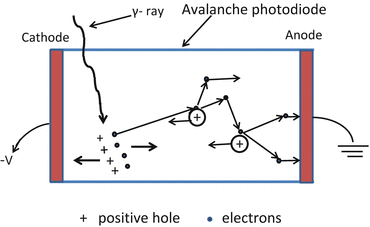
Fig. 2.3
The signal (gain of 1) is formed by the migration of electron–hole pair created by interaction of radiation with semiconductor material and significantly weaker than the PM tube signal (gain of 106–107). If, however, a reverse bias voltage of sufficient magnitude (200–2000 V) is applied, then the free electron accelerates in the material and can knock out an electron from an atomic orbital creating a second electron–hole pair and the process continues to create an avalanche phenomenon with signal gain of almost 100–1000. Such detectors are called avalanche photodiode (APD)
The APDs have been used in PET/MR scanners (see later), because PET signals from APDs are not affected by the magnetic field. A different variety of APDs are position-sensitive planar APDs (PS-APDs) which use signals from the four corners of the detector to ascertain the location of an event. However, PS-APDs suffer from worse noise. A newer APD is Geiger-mode APD or silicon photomultiplier (SiPM), which is made by connecting a series of micro-APD cells connected to bias voltage via individual resistor in the surrounding silicon. As in a Geiger detector, when photon interacts in the cell, it discharges and then is quenched through the resistor producing a single pulse. When SiPM is coupled to a scintillator, a large number of light photons produced by interaction of radiations from a source strike as many micro-APD cells. This produces an output pulse (gain of 105–107) as large as in conventional PM tubes. Research is continuing to improve this device.
Another category of semiconductor detectors like cadmium–zinc–tellurium (CZT) and cadmium–tellurium (CdTe) has relatively high stopping power and excellent energy resolution (~5%) and have potential for use in PET scanners. These detectors are fabricated by combining melted Cd and Te (and zinc for CZT) and heating until CdTe or CZT crystals are produced. Sometimes chlorine or indium is added as doping agent to improve the conductivity of detectors thus enhancing the spatial resolution and sensitivity. Although these detectors have been used in SPECT cameras, their use in PET camera is limited due to difficulty in fabricating larger crystals and poor timing performance. However, they are useful for small-animal PET scanner using small crystals providing good resolution of several millimeters. Shiga et al. (2009) made a comparative study between a PET scanner with CdTe detector and one with BGO detector and found better detectability with the former because of high spatial resolution and low scatter noise.
Photomultiplier Tube
As discussed briefly earlier, a PM tube is needed to convert the light photons produced in the detector by γ-ray interaction in the detector to an electrical pulse. The PM tube is a vacuum glass tube containing a photocathode at one end, ten dynodes in the middle, and an anode at the other end, as shown in Fig. 2.4. The photocathode is usually an alloy of cesium and antimony that releases electrons after absorption of light photons. The PM tube is fixed onto the detector by optical grease or optical light pipes.
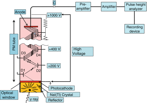
Fig. 2.4
A photomultiplier tube showing the photocathode at one end, several dynodes inside, and an anode at the other end
A high voltage of ∼1000 V is applied between the photocathode and the anode, with about 100-V increments between the dynodes. When light photons from the detector strike the photocathode of the PM tube, electrons are emitted, which are accelerated toward the next closest dynode by the voltage difference between the dynodes. Approximately 1–3 electrons are emitted per 7–10 light photons. Each of these electrons is again accelerated toward the next dynode and then more electrons are emitted. The process of multiplication continues until the last dynode is reached and a pulse of electrons is produced, which is attracted toward the anode. The pulse is then delivered to the preamplifier. Next, it is amplified by an amplifier to a detectable pulse, which is then analyzed for its size by the PHA, and finally delivered to a recorder or computer for storage or to a monitor for display. PM tubes are sturdy and expensive and provide fast and strong output pulse.
Pulse Height Analyzer
A PHA is a device that sorts out photons of different energies emitted by photons of the same or different radionuclides or from the scattered photons. Functionally, a PHA is a discriminator with a lower-level and an upper-level setting or with a baseline and a window above the baseline. In either setting, photons of selected energy only are accepted and others are rejected. This type of pulse sorting is essential in nuclear medicine imaging to count mainly unscattered photons that come out of the organ of interest for image formation. The narrower the window of the PHA, the more accurate is the energy discrimination of photons from the sample, but the detection efficiency is reduced. In the case of PET systems, the window of the PHA is centered on 511 keV, with a width of 350–650 keV.
Arrangement of Detectors
In the earlier designs of PET cameras, each detector (normally BGO) was glued to a single PM tube, and a large array of such detectors were arranged in multiple circular rings around the object of imaging. The axial field of view (FOV) is defined by the width of the array of the rings, and the number of detectors per ring varies with the manufacturers. The total number of detectors ranges in thousands, depending on the manufacturer. The larger the number of detectors and hence the more PM tubes per ring, the better the spatial resolution of the system. Although such systems provide good resolution, the cost of using many PM tubes is high, and packaging of a large number of detectors with PM tubes becomes impractical.
In current PET scanners, the block detectors are used, in which small detectors are created by partially cutting a large block of detector material and then are attached to a smaller number of PM tubes. Round or square PM tubes of 1–5 cm dimension are commonly used in PET scanners. A schematic block detector is shown in Fig. 2.5. Typically, a block detector of dimension 4 × 4 × 3 cm is grooved into an array of 6 × 8, 7 × 8 or 8 × 8 elements by making partial cuts through the crystal with a saw. The cuts are made at varying depths, with the deepest cut at the edge of the block. The grooves between the elements are filled with an opaque reflective material that prevents optical spillover between elements. Such uneven cutting results in linear sharing of light among PM tubes so that light from photon interaction in the corner element with deep cut will be detected by the PM tube located under that element, whereas the light from the middle interaction will be shared by all PM tubes. The width of the detector elements, among other factors, determines the spatial resolution of the imaging device and is normally 4–5 mm in modern PET scanners (see Chap. 6) The entire block detector is attached to several PM tubes (normally four PM tubes) in the same fashion as in scintillation cameras. BGO block detectors can use up to 16 detector elements per PM tube, whereas LSO block detectors use up to 144 detector elements because of higher intensity of scintillation emission. The detector elements are packed in 3–6 rings in a block. A typical commercial block detector is shown in Fig. 2.6. A PET scanner can contain many block detectors, the number of which varies with the manufacturer. The block detectors are arranged in arrays in full rings or partial rings in different configurations discussed later. The number of rings varies from 18 to 52 depending on the manufacturer. The block detector design has the advantage of reduced dead time compared with those of the scintillation cameras because of the restricted light spread in the former.
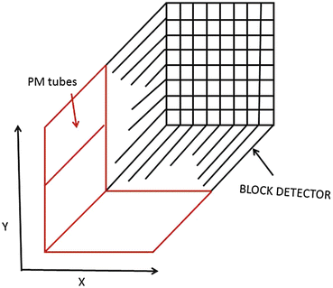
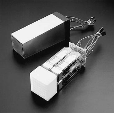
Fig. 2.5
A schematic block detector is segmented into 8 × 8 elements, and four PM tubes are coupled to the block for pulse formation
Fig. 2.6
A typical commercial block detector (8 × 8) attached to four square PM tubes (bottom) and a packaged module (top), developed and manufactured by Siemens Medical Solutions USA (Courtesy of CPS Innovations, Knoxville, TN, USA, currently Siemens Medical Solutions USA, Inc.)
A modification of the basic block detector has been made such that each PM tube straddles over four quadrants of four different blocks (Fig. 2.7). The technique of quadrant sharing permits the use of larger PM tubes and reduces the total number of PM tubes used in the PET system. This design improves the spatial resolution relative to the basic design but has the disadvantage of increasing the dead time.
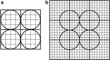
Fig. 2.7
Block detector illustrating the quadrant sharing of PM tubes. (a) PM tubes assigned in four quadrants separately. (b) Each PM tube shares four quadrants of four block detectors and improves the spatial resolution (Reprinted with the permission of the Cleveland Clinic Center for Medical Art and Photography © 2009. All rights reserved)
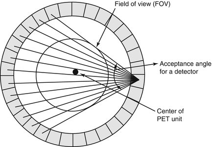
In PET scanners with block detectors, each detector pair is not connected by coincidence circuitry for practical difficulty, so the detectors are grouped together into banks or sets, which are then connected in coincidence opposite to each other. Essentially each detector in a set is connected by a coincidence circuit with a time window (see next section) to a set of opposite detectors (both in plane and axial). If there are N detectors in a ring, typically each detector can be connected in coincidence with N/2 detectors on the opposite side, and, therefore, N/2 “fan-beam” projections are available for each detector (Fig. 2.8). These fan-beam projections form for each detector an angle of acceptance in the transaxial plane, and these angles of acceptance for all detectors in the ring form the transaxial field of view (FOV). The larger the number of detectors (up to N/2) are in multicoincidence with each detector, the larger will be the angle of acceptance and hence the larger transaxial FOV for the PET system.